ChipApex | Global Electronic Components Supplier
SEARCH
Search Product
Search Post
— IC芯片 | 连接器 | 传感器 | 被动器件 —
Search productSearch post
— IC芯片 | 连接器 | 传感器 | 被动器件 —
Consult the customer manager about the wholesale price.
consultation hotline:86-132-6715-2157
email:[email protected]
Contact the product manager for consultation. One-stop consultation is available.
Do you want a lower wholesale price? Please send us your inquiry and we will reply immediately.
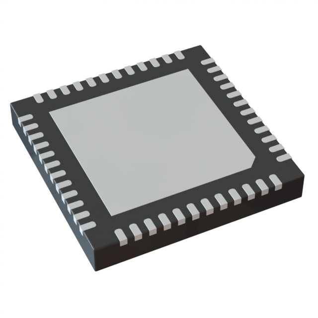
The MAX3638ETM2 is a low-jitter, wide frequency range programmable clock generator with 10 outputs. It features a phase-locked loop (PLL) and on-chip voltage-controlled oscillator (VCO) operating from 3.83GHz to 4.025GHz. The device provides nine differential LVDS/LVPECL outputs and one LVCMOS output across three banks. Input options include crystal, LVCMOS, or differential clocks. Key electrical parameters: supply voltage 3V to 3.6V; max frequency 800MHz; integrated jitter 0.34ps RMS (12kHz to 20MHz); operating temperature -40°C to +85°C. Package: 48-TQFN (7x7mm).
Verify the specific suffix 'ETM2' against official Microchip documentation to confirm package marking and tape-and-reel specifications. Ensure compatibility with existing board layouts regarding the 48-TQFN exposed pad thermal requirements.
Select based on required output interface types (LVDS vs. LVPECL) and frequency ranges up to 800MHz. Consider the pin-programmable divider settings for precise frequency synthesis. Ensure adequate power supply filtering for the VCC pin to maintain low jitter performance.
The MAX3638 series is designed for next-generation network equipment requiring robust high-speed data transmission. It replaces multiple crystal oscillators and clock distribution ICs, saving cost and space on system boards.
Publicly confirmed substitute part numbers are not available in the provided source material.
The differential LVDS/LVPECL outputs operate up to 800MHz.
The output interface for each bank (A, B, C) is individually programmed via dedicated control pins (QA_CTRL1, QA_CTRL2, QB_CTRL, QC_CTRL).
Integrated phase jitter is typically 0.34ps RMS (12kHz to 20MHz) and 0.14ps RMS (1.875MHz to 20MHz).
 MAX3638ETM2
The activity of extra discounts on wholesale prices is in full swing…
Please fill in your contact information and we will send you the latest wholesale price list.