ChipApex | Global Electronic Components Supplier

SEARCH
Search Product
Search Post
— IC芯片 | 连接器 | 传感器 | 被动器件 —
Search productSearch post
— IC芯片 | 连接器 | 传感器 | 被动器件 —
Consult the customer manager about the wholesale price.
consultation hotline:86-132-6715-2157
email:[email protected]
Contact the product manager for consultation. One-stop consultation is available.
Do you want a lower wholesale price? Please send us your inquiry and we will reply immediately.
MAX4019ESD+T is listed in the Instrumentation, Op Amps, Buffer Amps range at ChipApex. The manufacturer field lists Analog Devices Inc./Maxim Integrated. Its product description is IC BUFFER 3 CIRCUIT 14SOIC. Review the specifications below when checking this part for your BOM.
The MAX4019ESD+T is a precision, closed-loop buffer featuring four channels with internal resistors for fixed gains of +2 or -1. It operates from single supplies of +3.15V to +11V or dual supplies of ±1.575V to ±5.5V. The device provides rail-to-rail outputs and an input range extending 100mV beyond the negative rail. Key electrical parameters include a 200MHz small-signal bandwidth, 600V/µs slew rate, and 5.5mA quiescent current per channel. A disable feature reduces supply current to 400µA. It is housed in a 14-pin SO package.
Verify the specific suffix 'ESD' indicates the 14-pin SO package variant when sourcing. Confirm RoHS compliance status via official manufacturer documentation prior to integration. Ensure the enable pin logic levels match the system control voltages to prevent unintended activation or high standby current draw during disabled states.
Select this component for designs requiring multiple buffered channels with fixed gain configurations in a compact footprint. The integrated enable function supports power management strategies in battery-operated equipment. Consider the 14-pin SO package constraints regarding thermal dissipation and PCB layout requirements for high-frequency signal integrity compared to other family members like the MAX4014.
This part belongs to the MAX4014/MAX4017/MAX4019/MAX4022 family of low-cost, high-speed, single-supply buffers. While sharing core amplifier architecture, the MAX4019 specifically integrates four channels and includes individual enable pins for each buffer, distinguishing it from the two-channel MAX4017 and the unbuffered MAX4014.
MAX4017ESA+T
The device utilizes internal precision resistors configured to provide a closed-loop gain of +2V/V in non-inverting mode or -1V/V in inverting mode, eliminating the need for external feedback resistors.
Activating the disable feature via the EN_ pin reduces the quiescent supply current from approximately 5.5mA to 400µA per buffer, placing the device in a low-power state while maintaining high off-isolation.
Explore related parts through Amplifiers, Linear, Integrated Circuits (ICs), all product categories.
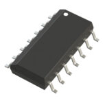 MAX4019ESD+T

The activity of extra discounts on wholesale prices is in full swing…
Please fill in your contact information and we will send you the latest wholesale price list.