ChipApex | Global Electronic Components Supplier

SEARCH
Search Product
Search Post
— IC芯片 | 连接器 | 传感器 | 被动器件 —
Search productSearch post
— IC芯片 | 连接器 | 传感器 | 被动器件 —
Consult the customer manager about the wholesale price.
consultation hotline:86-132-6715-2157
email:[email protected]
Contact the product manager for consultation. One-stop consultation is available.
Do you want a lower wholesale price? Please send us your inquiry and we will reply immediately.
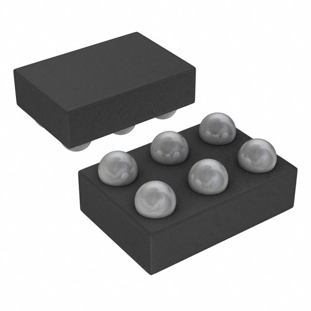
MAX44290ANT+T is listed in the Instrumentation, Op Amps, Buffer Amps range at ChipApex. The manufacturer field lists Analog Devices Inc./Maxim Integrated. Its product description is IC OPAMP GP 1 CIRCUIT 6WLP. Review the specifications below when checking this part for your BOM.
The MAX44290ANT+T is a single-channel operational amplifier in a 6-bump WLP package. It operates from a supply voltage of 1.8V to 5.5V, or 1.7V within the 0°C to +70°C range. Key electrical parameters include a 15MHz gain-bandwidth product, 7V/µs slew rate, and 750µA quiescent current. The device features rail-to-rail input and output capabilities with an input offset voltage of 50µV maximum at +25°C. Input bias current is 500fA typical, and input voltage noise density is 12.7nV/√Hz.
Verify the component designation matches the specific Analog Devices part number exactly. Confirm the package type corresponds to the 6-bump wafer-level configuration. Ensure the temperature rating aligns with the required operating environment specifications for the intended application design.
Select this component for designs requiring low-voltage operation down to 1.8V with precision signal conditioning. The ultra-low input bias current makes it suitable for interfacing with high-impedance sensors. The compact footprint supports space-constrained portable electronics where minimal board area is critical.
This device belongs to the MAX44290 series of low-power, high-speed operational amplifiers manufactured by Analog Devices. It is designed for applications demanding high dynamic range and precision in single-supply environments. The series emphasizes low noise and high input impedance characteristics.
No public confirmed substitute part numbers are available in the provided documentation.
It utilizes an internal charge pump that creates a voltage rail 1V above VDD to power the PMOS input differential pair, removing the crossover distortion found in standard CMOS structures.
The device recovers from shutdown in less than 30µs without requiring self-calibration, retaining its power-up trim settings.
Explore related parts through Amplifiers, Linear, Integrated Circuits (ICs), all product categories.
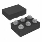 MAX44290ANT+T

The activity of extra discounts on wholesale prices is in full swing…
Please fill in your contact information and we will send you the latest wholesale price list.