 ChipApex | Global Electronic Components Supplier

SEARCH
Search Product
Search Post
— IC芯片 | 连接器 | 传感器 | 被动器件 —
Search productSearch post
— IC芯片 | 连接器 | 传感器 | 被动器件 —
Consult the customer manager about the wholesale price.
consultation hotline:86-132-6715-2157
email:[email protected]
Contact the product manager for consultation. One-stop consultation is available.
Do you want a lower wholesale price? Please send us your inquiry and we will reply immediately.
The MAX6033CAUT50#TG16 is a high-precision series voltage reference with a fixed output of 5.000V and an initial accuracy of ±0.1%. It features a maximum temperature coefficient of 40ppm/°C over the -40°C to +125°C automotive range. The device operates within a supply voltage range of 5.2V to 12.6V, consuming a typical quiescent current of 40µA while sourcing up to 15mA. Packaged in a compact SOT-23-6 surface-mount format, it includes separate force (OUTF) and sense (OUTS) outputs for improved regulation.
Verify the specific suffix #TG16 against official manufacturer documentation to confirm RoHS compliance status and lead-free specifications. Confirm that the 'T' designation corresponds to tape and reel packaging requirements for your automated assembly line. Ensure the component meets the required automotive temperature grade (-40°C to +125°C) for your specific application environment before finalizing procurement.
Select this part when a stable 5V reference is needed with moderate precision (±0.1%) and low cost. It is suitable for applications where the input voltage exceeds the output by at least 200mV. Consider alternative family members if tighter temperature coefficients or higher initial accuracies are required, as those options may consume more power or require different input voltage ranges.
This component belongs to the MAX6033 family of ultra-high-precision series voltage references manufactured by Analog Devices / Maxim Integrated. The family offers various output voltages and accuracy grades, all sharing a common miniature SOT-23 package and low-power architecture designed for battery-operated and space-constrained electronic designs.
Direct substitutes include other MAX6033 variants such as MAX6033BAUT50+T or MAX6033AAUT50-T, which share the same pinout and package but offer different accuracy and temperature coefficient specifications. Verify that any replacement maintains the required 5V output and fits within the available input voltage headroom.
The device is designed to remain stable with capacitive loads, including bypass capacitance, of up to 100µF.
The OUTS pin serves as the voltage reference sense output. It should be connected to the load to compensate for voltage drops in the trace between the OUTF pin and the load.
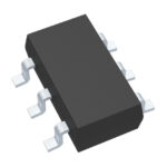 MAX6033CAUT50#TG16

The activity of extra discounts on wholesale prices is in full swing…
Please fill in your contact information and we will send you the latest wholesale price list.







