 ChipApex | Global Electronic Components Supplier

SEARCH
Search Product
Search Post
— IC芯片 | 连接器 | 传感器 | 被动器件 —
Search productSearch post
— IC芯片 | 连接器 | 传感器 | 被动器件 —
Consult the customer manager about the wholesale price.
consultation hotline:86-132-6715-2157
email:[email protected]
Contact the product manager for consultation. One-stop consultation is available.
Do you want a lower wholesale price? Please send us your inquiry and we will reply immediately.
The MAX6071BAUT25/V+T is a low-noise, high-precision series voltage reference manufactured by Analog Devices Inc./Maxim Integrated. It provides a fixed output voltage of 2.5V with an initial accuracy of ±0.08% and a maximum temperature drift of 8ppm/°C. The device operates within an input voltage range of 2.8V to 5.5V and consumes a typical supply current of 150µA. It supports bidirectional load currents up to 10mA and features a shutdown mode with reduced current consumption. The component is housed in a compact 6-pin SOT-23 package and is specified for operation across the extended industrial temperature range of -40°C to +125°C.
Verify the specific suffix '/V+' against official documentation to confirm automotive qualification status or environmental compliance details. Confirm package type and availability through authorized distributors as stock levels fluctuate. Ensure the ordering code matches the required grade and output voltage variant before procurement.
Select this component when a fixed 2.5V reference with B-grade accuracy is required. Consider the MAX6070 if a filter option for wideband noise reduction is needed. Evaluate the WLP package option if board space constraints are critical. Verify that the input voltage range accommodates the system's supply variations.
This part belongs to the MAX6070/MAX6071 family of low-noise, high-precision series voltage references. The MAX6071 variant distinguishes itself from the MAX6070 by lacking the internal filter capacitor option, offering faster settling times. Both families share similar electrical characteristics and packaging options, designed for high-accuracy applications.
MAX6070BAUT25+T: Similar specifications but includes a filter option for lower wideband noise.
The MAX6070 includes a filter input pin for reducing high-frequency noise, while the MAX6071 does not have this feature and typically offers faster turn-on and enable settling times.
The MAX6071 provides separate Force (OUTF) and Sense (OUTS) outputs. Connecting OUTS to the load ground allows the device to compensate for voltage drops across PCB traces, ensuring accurate voltage delivery at the load.
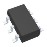 MAX6071BAUT25/V+T

The activity of extra discounts on wholesale prices is in full swing…
Please fill in your contact information and we will send you the latest wholesale price list.





