 ChipApex | Global Electronic Components Supplier

SEARCH
Search Product
Search Post
— IC芯片 | 连接器 | 传感器 | 被动器件 —
Search productSearch post
— IC芯片 | 连接器 | 传感器 | 被动器件 —
Consult the customer manager about the wholesale price.
consultation hotline:86-132-6715-2157
email:[email protected]
Contact the product manager for consultation. One-stop consultation is available.
Do you want a lower wholesale price? Please send us your inquiry and we will reply immediately.
The MAX6133BASA41+ is a high-precision, low-power, low-dropout series voltage reference manufactured by Analog Devices Inc./Maxim Integrated. It provides a fixed output voltage of 4.096V with an initial accuracy of ±0.08% and a maximum temperature coefficient of 5ppm/°C across the -40°C to +125°C operating range. The device operates within an input voltage range of 4.2V to 12.6V, consuming a typical quiescent supply current of 40µA. It features a maximum dropout voltage of 0.4V at 10mA load and supports a source current up to 15mA. Packaged in an 8-pin SOIC (SO-Narrow-8), it utilizes bandgap technology for stability.
Verify the specific suffix 'B' indicates the B-grade tolerance class with ±0.08% initial accuracy and 5ppm/°C max temperature coefficient. Confirm the 'SA' designation corresponds to the SO-Narrow-8 package variant. Ensure the '41' suffix matches the required 4.096V output voltage option. Check datasheet revisions for any updates to electrical characteristics or thermal performance data.
Select this component when a fixed 4.096V reference is required with strict accuracy constraints. The B-grade specification suits applications tolerating slightly wider drift than A-grade parts while maintaining low power consumption. Consider the 15mA source current limit for load requirements. Evaluate the 8-pin SO package footprint against available PCB space constraints.
This part belongs to the MAX6133 family of precision voltage references designed for portable and communication applications. It shares architectural similarities with other Maxim series references but distinguishes itself through its specific combination of low dropout voltage and ultra-low supply current. The family includes variants with different output voltages and package options to support diverse design needs.
Public confirmed substitute part numbers are not provided in the source material.
The device guarantees load regulation specifications for source currents up to 15mA.
Thermal hysteresis is defined as the change in output voltage after cycling from maximum to minimum temperature, with a typical value of 120ppm caused by differential package stress.
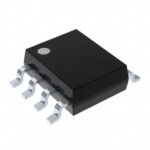 MAX6133BASA41+

The activity of extra discounts on wholesale prices is in full swing…
Please fill in your contact information and we will send you the latest wholesale price list.





