 ChipApex | Global Electronic Components Supplier

SEARCH
Search Product
Search Post
— IC芯片 | 连接器 | 传感器 | 被动器件 —
Search productSearch post
— IC芯片 | 连接器 | 传感器 | 被动器件 —
Consult the customer manager about the wholesale price.
consultation hotline:86-132-6715-2157
email:[email protected]
Contact the product manager for consultation. One-stop consultation is available.
Do you want a lower wholesale price? Please send us your inquiry and we will reply immediately.
The MAX6174AASA+ is a high-precision voltage reference providing a fixed +4.096V output. It features a maximum temperature coefficient of 3ppm/°C and an initial accuracy of ±0.06%. The device accepts input voltages from 6.1V to 40V, draws 500µA maximum supply current, and sources up to 30mA. It includes a TEMP pin for die temperature sensing and a TRIM pin for fine adjustment. Operating over -40°C to +125°C, it uses band-gap technology and requires no output bypass capacitor for stability.
Verify the specific suffix against official documentation to confirm package type and RoHS compliance status. Confirm that the ordering code matches the required output voltage and accuracy grade. Check for AEC-Q100 qualification if automotive reliability is required, as this may involve a distinct /V suffix variant. Ensure the component meets the specified thermal operating range for the target environment.
Select this component when a stable 4.096V reference is needed with minimal temperature drift. The integrated temperature sensor allows for simultaneous ambient monitoring. Consider the 30mA source capability for driving moderate loads directly. Verify that the input voltage remains within the guaranteed regulation range relative to the output level.
This part belongs to the MAX6173–MAX6177 family of high-precision voltage references. All members share identical architectures, featuring curvature correction and temperature outputs. They differ primarily in their factory-preset output voltages, which include 2.5V, 3.3V, 4.096V, 5.0V, and 10V options. The family maintains consistent performance characteristics across all variants.
Other members of the MAX6173–MAX6177 series offer different preset voltages but share the same package and functional interface. Direct substitutes must match the 4.096V output requirement. Verify pin compatibility and thermal specifications before integrating alternative components.
No, the device does not require an output bypass capacitor for stability and is stable with capacitive loads up to 100μF.
The output voltage is trimmed by connecting a resistive divider network between the OUT, TRIM, and GND pins.
The TEMP pin provides an output voltage that is linearly proportional to the internal die temperature.
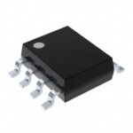 MAX6174AASA+

The activity of extra discounts on wholesale prices is in full swing…
Please fill in your contact information and we will send you the latest wholesale price list.






