 ChipApex | Global Electronic Components Supplier

SEARCH
Search Product
Search Post
— IC芯片 | 连接器 | 传感器 | 被动器件 —
Search productSearch post
— IC芯片 | 连接器 | 传感器 | 被动器件 —
Consult the customer manager about the wholesale price.
consultation hotline:86-132-6715-2157
email:[email protected]
Contact the product manager for consultation. One-stop consultation is available.
Do you want a lower wholesale price? Please send us your inquiry and we will reply immediately.
The MAX6225AESA+ is a low-noise, precision buried-zener voltage reference providing a fixed 2.500V output in an 8-pin SO package. It operates within an extended temperature range of -40°C to +85°C with a maximum temperature coefficient of 3ppm/°C and ±0.02% initial accuracy. The device supports input voltages from 8V to 36V, draws approximately 1.8mA supply current, and delivers up to 15mA source/sink current. Key electrical characteristics include 1.5µVp-p noise (0.1Hz to 10Hz), 20ppm/1000h long-term stability, and excellent line/load regulation.
Verify the specific suffix 'E' confirms the -40°C to +85°C operating range and 'S' indicates the 8-pin SO package. Confirm the '+' suffix denotes lead-free/RoHS compliance as per manufacturer specifications. Ensure the ordering code matches the required temperature coefficient grade and initial accuracy tolerance before procurement.
Select this component when designing high-resolution data-conversion systems requiring low drift and minimal noise. Consider the 8V to 36V input range and 15mA load capability for system power budgeting. Evaluate the need for external trimming or noise reduction features based on specific application requirements.
Part of the MAX6225/MAX6241/MAX6250 family of low-noise precision voltage references. The MAX6225 variant specifically provides a 2.500V output, while other family members offer 4.096V or 5.000V outputs. All share similar buried-zener architecture and performance characteristics.
Direct replacements within the same series include MAX6225AEPA+ (Plastic DIP) or MAX6225ACSA+ (SO, commercial temp). Verify package compatibility and temperature range alignment when substituting.
Add a 1μF capacitor to the NR (Noise Reduction) pin to augment wideband noise reduction.
Yes, the device is stable with capacitive load values ranging from 0μF to 100μF for all load currents.
Yes, the output voltage can be trimmed by connecting a potentiometer between OUT and GND, with the tap connected to the TRIM pin.
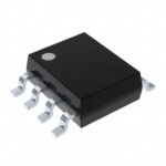 MAX6225AESA+

The activity of extra discounts on wholesale prices is in full swing…
Please fill in your contact information and we will send you the latest wholesale price list.







