 ChipApex | Global Electronic Components Supplier
SEARCH
Search Product
Search Post
— IC芯片 | 连接器 | 传感器 | 被动器件 —
Search productSearch post
— IC芯片 | 连接器 | 传感器 | 被动器件 —
Consult the customer manager about the wholesale price.
consultation hotline:86-132-6715-2157
email:[email protected]
Contact the product manager for consultation. One-stop consultation is available.
Do you want a lower wholesale price? Please send us your inquiry and we will reply immediately.
The MAX6389LT31D3+T is a dual microprocessor supervisory circuit from the MAX6381–MAX6390 family, designed for low-voltage and low-power applications. It monitors two power-supply inputs within a range of +1.8V to +5.0V while consuming only 3µA of supply current at +1.8V. The device features a factory-set reset threshold voltage of 3.08V with an accuracy of 2.5%. It provides an active-low, open-drain reset output that asserts when VCC falls below the threshold and remains asserted for a minimum timeout period of 280ms after VCC rises above the threshold. The component operates over an extended temperature range from -40°C to +125°C and is housed in a compact SC-70-4 package.
Verify the exact suffix D3+T against the manufacturer's official datasheet to confirm the specific package variant and tape-and-reel configuration. Ensure the lead-free status aligns with RoHS compliance requirements for your assembly process. Cross-reference the threshold voltage code to guarantee the 3.08V specification matches your design needs before finalizing procurement orders.
Select this component when dual voltage monitoring is required in a minimal footprint. The open-drain output allows for wired-OR configurations or level shifting. Consider the 280ms delay for system startup stability. Verify that the 3.08V threshold adequately covers the brown-out protection requirements for the monitored rails without causing nuisance resets during normal operation fluctuations.
This part belongs to the MAX6389 series of single and dual low-voltage, low-power µP reset circuits. The series offers various threshold voltages and timeout delays to accommodate different system architectures. The LT suffix typically denotes the specific threshold voltage setting, while D3 indicates the SC-70-4 package type. This family is widely used in consumer electronics and industrial applications where space and power efficiency are critical constraints.
Check for MAX6389XS31D3+T if adjustable thresholds are needed instead of fixed settings. Verify pinout compatibility with existing PCB layouts when substituting. Confirm that the replacement maintains the same active-low open-drain output characteristic and 280ms timeout delay to ensure system behavior remains unchanged.
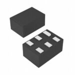 MAX6389LT31D3+T
The activity of extra discounts on wholesale prices is in full swing…
Please fill in your contact information and we will send you the latest wholesale price list.





