 ChipApex | Global Electronic Components Supplier
MAX840ISA+T
Search Product
Search Post
— IC芯片 | 连接器 | 传感器 | 被动器件 —
Search productSearch post
— IC芯片 | 连接器 | 传感器 | 被动器件 —
Consult the customer manager about the wholesale price.
consultation hotline:86-132-6715-2157
email:[email protected]
Contact the product manager for consultation. One-stop consultation is available.
Do you want a lower wholesale price? Please send us your inquiry and we will reply immediately.
The MAX840ISA+T is a charge pump integrated circuit designed for cellular telephone transmitter applications. It generates regulated negative output voltages, specifically -2V and adjustable ranges from -0.5V to -9.4V, from a single 2.5V to 10V supply input. The device operates in the industrial temperature range of -40°C to +85°C and is housed in an 8-pin SOIC package.
Verify the exact suffix against the manufacturer's current datasheet to confirm pinout and electrical specifications. Ensure the component meets the required operating temperature range for the intended environment. Cross-reference the ordering information with official Analog Devices documentation to avoid counterfeit parts.
Select this component when a compact solution is needed to generate stable negative bias voltages from a single positive rail. It is suitable for space-constrained mobile designs requiring efficient charge pump topology without external inductors. Consider the output current requirements and input voltage range compatibility with the system power supply.
This part belongs to the Maxim Integrated family of charge pump regulators, specialized for portable wireless communication devices. It addresses the need for negative bias supplies in RF circuits where multiple voltage rails are typically unavailable or inefficient to generate using linear regulators.
Check for direct pin-to-pin replacements within the MAX840 series or newer generations from Analog Devices. Verify that any substitute maintains the same output voltage characteristics and package dimensions.
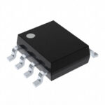 MAX840ISA+T
The activity of extra discounts on wholesale prices is in full swing…
Please fill in your contact information and we will send you the latest wholesale price list.





