 ChipApex | Global Electronic Components Supplier

SEARCH
Search Product
Search Post
— IC芯片 | 连接器 | 传感器 | 被动器件 —
Search productSearch post
— IC芯片 | 连接器 | 传感器 | 被动器件 —
Consult the customer manager about the wholesale price.
consultation hotline:86-132-6715-2157
email:[email protected]
Contact the product manager for consultation. One-stop consultation is available.
Do you want a lower wholesale price? Please send us your inquiry and we will reply immediately.
MAX9310AEUP+T is listed in the Clock Buffers, Drivers range at ChipApex. The manufacturer field lists Analog Devices Inc./Maxim Integrated. Its product description is IC CLK BUFFER 2:5 1GHZ 20TSSOP. Review the specifications below when checking this part for your BOM.
The MAX9310AEUP+T is a high-speed clock buffer and distribution circuit manufactured by Analog Devices Inc./Maxim Integrated. It features a 2:5 fanout ratio, converting two differential inputs into five LVDS outputs. The device supports HSTL and LVPECL input standards and operates within a supply voltage range of 3V to 3.6V. Designed for surface mount applications, it is housed in a 20-TSSOP package with a width of 4.40mm. The component is rated for an operating temperature range of -40°C to +85°C and supports maximum frequencies up to 1 GHz.
Verify the specific suffix 'A' and '+T' against official documentation to confirm temperature grade and tape & reel packaging status. Ensure the 20-TSSOP footprint matches the target PCB design. Confirm RoHS compliance details through the manufacturer's current datasheet before finalizing procurement specifications.
Select this component when a 2-to-5 differential fanout is required for LVDS loads. It is suitable for designs needing HSTL or LVPECL compatibility at speeds up to 1 GHz. Ensure the system power supply remains strictly between 3V and 3.6V. Consider the 20-TSSOP package constraints for thermal management and board space availability.
This part belongs to the Maxim Integrated family of high-speed clock buffers. It serves as a distribution element for differential clock signals in mixed-signal environments. The device integrates level shifting capabilities to interface between various logic families and LVDS output stages efficiently.
Consult official cross-reference lists for verified substitutes. Generic buffer replacements may not match the specific 2:5 ratio or input/output voltage levels. Verify pin compatibility and electrical characteristics before substituting.
Explore related parts through Clock/Timing, Integrated Circuits (ICs), all product categories, ChipApex homepage.
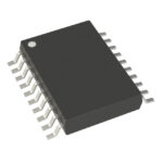 MAX9310AEUP+T

The activity of extra discounts on wholesale prices is in full swing…
Please fill in your contact information and we will send you the latest wholesale price list.





