 ChipApex | Global Electronic Components Supplier

SEARCH
Search Product
Search Post
— IC芯片 | 连接器 | 传感器 | 被动器件 —
Search productSearch post
— IC芯片 | 连接器 | 传感器 | 被动器件 —
Consult the customer manager about the wholesale price.
consultation hotline:86-132-6715-2157
email:[email protected]
Contact the product manager for consultation. One-stop consultation is available.
Do you want a lower wholesale price? Please send us your inquiry and we will reply immediately.
MAX9323EUP+T is listed in the Clock Buffers, Drivers range at ChipApex. The manufacturer field lists Analog Devices Inc./Maxim Integrated. Its product description is IC CLK BUFFER 1:4 1.5GHZ 20TSSOP. Review the specifications below when checking this part for your BOM.
The MAX9323EUP+T is a low-skew, low-jitter clock and data driver manufactured by Analog Devices Inc./Maxim Integrated. It distributes one of two single-ended LVCMOS inputs to four differential LVPECL outputs. The device operates from a 3.0V to 3.6V supply voltage, making it suitable for 3.3V systems. It features a logic control signal (CLK_SEL) to select the input signal distributed to all outputs. The component is housed in a 20-TSSOP package with an operating temperature range of -40°C to +85°C.
Verify the manufacturer designation as Analog Devices Inc./Maxim Integrated. Confirm the package type is 20-TSSOP with Tape & Reel (TR) packaging. Ensure the operating temperature range matches -40°C to +85°C. Check that the supply voltage range is 3.0V to 3.6V. Validate the frequency-max specification of 1.5 GHz against project requirements.
Select this component when a low-skew, low-jitter solution is required for distributing LVCMOS signals to LVPECL loads. It is ideal for 3.3V systems due to its specific supply voltage range. Consider the 20-TSSOP package size for surface mount applications. Ensure the design supports the 1.5 GHz maximum frequency capability.
This part belongs to the Clock Buffers, Drivers category. It functions as a fanout buffer, multiplexer, and data driver. The 1:4 ratio allows for efficient clock distribution from a single source to multiple destinations. The device integrates input selection logic to manage dual LVCMOS inputs.
Public confirmed substitute part numbers are not available in the provided documentation. Verify compatibility with existing circuit designs before considering alternative components.
Explore related parts through Clock/Timing, Integrated Circuits (ICs), all product categories, ChipApex homepage.
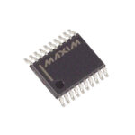 MAX9323EUP+T

The activity of extra discounts on wholesale prices is in full swing…
Please fill in your contact information and we will send you the latest wholesale price list.




