 ChipApex | Global Electronic Components Supplier
SEARCH
Search Product
Search Post
— IC芯片 | 连接器 | 传感器 | 被动器件 —
Search productSearch post
— IC芯片 | 连接器 | 传感器 | 被动器件 —
Consult the customer manager about the wholesale price.
consultation hotline:86-132-6715-2157
email:[email protected]
Contact the product manager for consultation. One-stop consultation is available.
Do you want a lower wholesale price? Please send us your inquiry and we will reply immediately.
The MAX951EPA is an ultra-low-power, single-supply integrated circuit combining a micro-power operational amplifier, a comparator, and a precision reference within an 8-pin plastic DIP package. It operates from a supply voltage range of 2.7V to 7V with a typical supply current of 7μA. The device features rail-to-rail output swing for both the op amp and comparator, ensuring compatibility with ground-referenced signals. The internal comparator includes ±3mV hysteresis for clean switching, while the op amp is unity-gain stable with a 20kHz gain bandwidth.
Verify the specific temperature grade and package variant when sourcing replacements, as the MAX951 series offers multiple options including military-grade CERDIP packages. Confirm that the target application does not require bypassing the reference output, as this may affect stability. Ensure board layout minimizes leakage currents due to the high-impedance CMOS inputs.
Select the MAX951EPA when a unified solution for signal amplification, threshold detection, and voltage referencing is required in space-constrained designs. This part is ideal for applications demanding minimal quiescent current without sacrificing rail-to-rail performance. Consider external hysteresis if the internal ±3mV band is insufficient for the specific noise environment.
This component belongs to the MAX951–MAX954 family of ultra-low-power mixed-signal ICs manufactured by Analog Devices / Maxim Integrated. The family differentiates models based on op amp gain stability and the presence of an internal reference. The MAX951 specifically integrates a unity-gain stable op amp with a precision 1.2V reference, distinguishing it from decompensated variants or those without internal references.
Direct pin-compatible alternatives within the same family include the MAX951ESA (SO package) and MAX951EUA (µMAX package). For broader replacements, verify that substitute parts maintain the 2.7V to 7V supply range and 7μA typical current consumption to ensure equivalent battery life performance.
Yes, the common-mode input voltage range extends from the negative supply rail (VSS), allowing the op amp and comparator to accept signals at ground.
The internal ±3mV hysteresis prevents output oscillation caused by noise or slow-moving input signals, ensuring clean switching transitions.
No, the datasheet explicitly states not to bypass the reference output. It is stable for capacitive loads less than 100pF, but adding a bypass capacitor may cause instability.
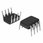 MAX951EPA
The activity of extra discounts on wholesale prices is in full swing…
Please fill in your contact information and we will send you the latest wholesale price list.





