 ChipApex | Global Electronic Components Supplier
SEARCH
Search Product
Search Post
— IC芯片 | 连接器 | 传感器 | 被动器件 —
Search productSearch post
— IC芯片 | 连接器 | 传感器 | 被动器件 —
Consult the customer manager about the wholesale price.
consultation hotline:86-132-6715-2157
email:[email protected]
Contact the product manager for consultation. One-stop consultation is available.
Do you want a lower wholesale price? Please send us your inquiry and we will reply immediately.
The MAX951ESA+ is an ultra-low-power, single-supply integrated circuit combining a micro-power operational amplifier, a comparator, and a precision reference within an 8-pin SOIC package. It operates from a supply voltage range of 2.7V to 7V with a typical supply current of 7μA. The device features rail-to-rail input and output capabilities, internal ±3mV comparator hysteresis for clean switching, and a 1.2V ±2% bandgap reference. Designed for battery-powered applications, it maintains excellent DC characteristics across the -40°C to +85°C temperature range.
Verify the specific suffix 'ESA' confirms the 8-pin SOIC package and industrial temperature range (-40°C to +85°C). Confirm RoHS compliance status via the manufacturer's latest documentation, as ordering suffixes may indicate environmental certifications. Ensure the design accounts for the single-supply operation requirements specified in the datasheet.
Select the MAX951ESA+ when a combined solution for amplification, threshold detection, and voltage referencing is required in space-constrained designs. It is ideal for high-impedance sensor buffering due to low input bias current. Consider the unity-gain stability of the op amp section for direct feedback configurations without external compensation components.
This component belongs to the MAX951–MAX954 family of ultra-low-power mixed-signal ICs manufactured by Analog Devices Inc./Maxim Integrated. The family differentiates models based on op amp gain stability (unity-gain vs. decompensated) and the presence of an internal reference. The MAX951 specifically integrates the reference and unity-gain stable op amp.
Official substitutes within the same family include the MAX952ESA+, which offers a decompensated op amp option for higher bandwidth applications while retaining the reference and comparator functions.
The REF pin provides access to the internal 1.2V ±2% bandgap reference voltage. On the MAX951, this reference is also internally connected to the inverting input of the comparator.
Power-supply bypass capacitors are not strictly required if the supply impedance is low, but it is good practice to bypass VDD with a 0.1μF capacitor to ground. The reference output should not be bypassed.
The internal ±3mV hysteresis increases noise immunity and ensures clean output switching even when processing slow-moving input signals, minimizing parasitic feedback through the power supplies.
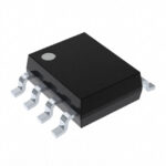 MAX951ESA+
The activity of extra discounts on wholesale prices is in full swing…
Please fill in your contact information and we will send you the latest wholesale price list.







