ChipApex | Global Electronic Components Supplier

SEARCH
Search Product
Search Post
— IC芯片 | 连接器 | 传感器 | 被动器件 —
Search productSearch post
— IC芯片 | 连接器 | 传感器 | 被动器件 —
Consult the customer manager about the wholesale price.
consultation hotline:86-132-6715-2157
email:[email protected]
Contact the product manager for consultation. One-stop consultation is available.
Do you want a lower wholesale price? Please send us your inquiry and we will reply immediately.
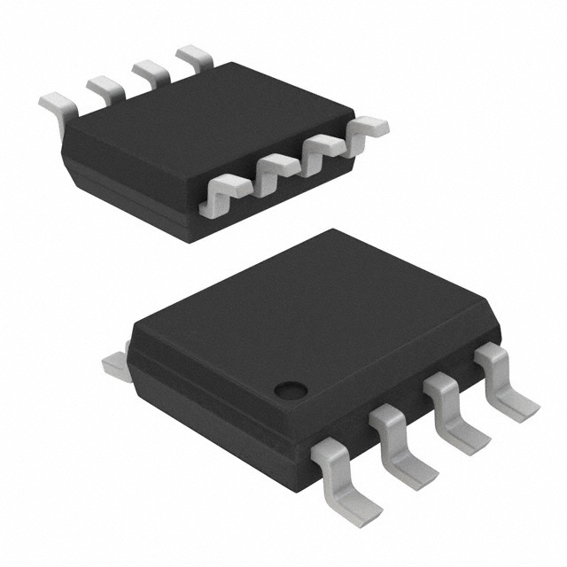
MB85RC1MTPNF-G-JNE1 is listed in the Memory IC range at ChipApex. The manufacturer field lists RAMXEED. Its product description is IC FRAM 1MBIT I2C 8SOP. Review the specifications below when checking this part for your BOM.
The MB85RC1MTPNF-G-JNE1 is a 1 Mbit (128 K x 8) Ferroelectric Random Access Memory (FeRAM) integrated circuit manufactured by RAMXEED. It utilizes a two-wire serial I2C interface and operates within a supply voltage range of 1.8 V to 3.6 V. The device supports clock frequencies up to 3.4 MHz in High Speed Mode and 1 MHz in Fast Mode Plus. It features a write endurance of at least 10^13 cycles per byte and data retention exceeding 10 years at +85°C. The component is housed in an 8-pin plastic SOP package with a lead pitch of 1.27 mm.
Verify the specific ordering suffix JNE1 corresponds to the tube packaging format required for your assembly process. Confirm that the manufacturer designation RAMXEED aligns with your approved vendor list, as this entity succeeded Fujitsu Semiconductor Memory Solutions Limited. Ensure compliance with RoHS and REACH regulations applicable to your region before finalizing procurement orders.
Select this component when a design requires high write endurance and fast access times without the latency associated with Flash memory polling. The I2C interface is suitable for space-constrained designs where fewer pins are available compared to SPI alternatives. Consider the 1.8 V to 3.6 V operating range to ensure compatibility with the system's logic levels and power rails.
This part belongs to the MB85RC1MT family of FeRAM devices from RAMXEED. The manufacturer continues to support existing product lines originally developed by Fujitsu Semiconductor Memory Solutions Limited under the same part numbering scheme. The technology leverages ferroelectric processes combined with silicon gate CMOS for reliable nonvolatile data storage.
MB85RC1MTPNF-G-JNERE1
No, the device does not require an acknowledge polling sequence. Write operations complete immediately upon the stop condition, unlike EEPROM or Flash memory which typically require wait times.
The device address is configured using external hardware connections to pins A1 and A2. These pins allow up to four devices to be connected to the same I2C bus by setting unique combinations of high or low logic levels.
The WP (Write Protect) pin disables write operations when held at a high level. When low or left open (internally pulled down), it allows the entire memory array to be overwritten. Reading is always enabled regardless of the WP state.
Explore related parts through Memory, Integrated Circuits (ICs), all product categories, ChipApex homepage.
 MB85RC1MTPNF-G-JNE1

The activity of extra discounts on wholesale prices is in full swing…
Please fill in your contact information and we will send you the latest wholesale price list.