 ChipApex | Global Electronic Components Supplier
SEARCH
Search Product
Search Post
— IC芯片 | 连接器 | 传感器 | 被动器件 —
Search productSearch post
— IC芯片 | 连接器 | 传感器 | 被动器件 —
Consult the customer manager about the wholesale price.
consultation hotline:86-132-6715-2157
email:[email protected]
Contact the product manager for consultation. One-stop consultation is available.
Do you want a lower wholesale price? Please send us your inquiry and we will reply immediately.
The MC100E196FNG is a 5V/EnECL Programmable Delay Chip (PDC) manufactured by onsemi in a PLCC-28 package. It provides a worst-case delay range of 2.0 ns with an approximate 20 ps per step resolution. The device supports PECL mode (VCC = 4.2 V to 5.7 V, VEE = 0 V) and NECL mode (VCC = 0 V, VEE = -4.2 V to -5.7 V). It features a linear FTUNE input for finer analog tuning, internal cascade circuitry for multi-chip expansion, and operates within a temperature range of 0°C to +85°C.
Verify the specific ordering suffix 'FNG' indicates a lead-free PLCC-28 package configuration. Confirm that the moisture sensitivity level aligns with the storage and handling requirements for Pb-Free components. Ensure the procurement source provides valid RoHS compliance documentation matching the manufacturer's specifications.
Select this component when precise differential edge placement is required using EnECL logic levels. The inclusion of the FTUNE pin distinguishes it from the MC100E195, offering enhanced resolution capabilities. Consider the cascading architecture if the application demands a programmable delay range exceeding the single-device maximum.
This part belongs to the MC10E/100E196 series of programmable delay chips designed for accurate timing control. The 100 Series variant includes temperature compensation compared to the standard 10 Series. It serves as a specialized timing element within clock distribution networks requiring fine-grained delay adjustments.
The MC100E195 is a related device lacking the FTUNE analog tuning feature. Substitution requires evaluating whether the additional analog resolution provided by the FTUNE pin is necessary for the specific application timing constraints.
The FTUNE pin applies an analog voltage to an internal linear ramp, reducing the minimum 20 ps digital LSB resolution further. This allows for finer delay adjustments beyond the discrete digital steps.
The D7 input serves as the cascade control signal. When asserted, it enables the chaining of multiple PDCs to increase the total programmable delay range without requiring external gating logic.
If the VBB pin is not utilized for AC coupling or as a switching reference, it should be left open. If used, it must be decoupled via a 0.01 µF capacitor and current limited to 0.5 mA.
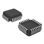 MC100E196FNG
The activity of extra discounts on wholesale prices is in full swing…
Please fill in your contact information and we will send you the latest wholesale price list.






