 ChipApex | Global Electronic Components Supplier

SEARCH
Search Product
Search Post
— IC芯片 | 连接器 | 传感器 | 被动器件 —
Search productSearch post
— IC芯片 | 连接器 | 传感器 | 被动器件 —
Consult the customer manager about the wholesale price.
consultation hotline:86-132-6715-2157
email:[email protected]
Contact the product manager for consultation. One-stop consultation is available.
Do you want a lower wholesale price? Please send us your inquiry and we will reply immediately.
MC100E416FN is listed in the Specialty Logic range at ChipApex. The manufacturer field lists onsemi. Its product description is IC LINE RCVR QUINT DIFF 28-PLCC. Review the specifications below when checking this part for your BOM.
The MC100E416FN is a 5-bit differential line receiver from the onsemi MC100 series, housed in a 28-lead PLCC package. It features high-frequency outputs with 2.0 GHz bandwidth and incorporates two internal stages of gain. The device supports PECL mode (VCC = 4.2 V to 5.7 V) and NECL mode (VEE = -4.2 V to -5.7 V). Key electrical parameters include a maximum propagation delay of 600 ps, an operating temperature range of 0°C to +85°C, and ESD protection exceeding 2 kV (HBM).
Verify the specific suffix 'FN' corresponds to the standard PLCC-28 package configuration as documented in the datasheet ordering information. Confirm whether the required unit is the lead-free variant (FNG) or the standard version based on project specifications. Ensure all VCC, VCCO, and VEE pins are externally connected to power supplies during validation to guarantee proper operation.
Select this component when a 5-channel differential receiver with integrated gain is required for high-frequency signal processing. The MC100 series offers temperature compensation compared to the MC10 series. Consider the 28-lead PLCC footprint for PCB layout compatibility. Verify that the system operates within the specified PECL or NECL voltage ranges and thermal limits.
This device belongs to the MC10E416/MC100E416 family of 5V/EnECL quint differential line receivers manufactured by onsemi. The MC100 series specifically includes temperature compensation features not present in the base MC10 series. The part is designed for robust performance in demanding high-speed digital environments requiring precise timing and signal integrity.
MC10E416FN serves as the non-temperature-compensated equivalent within the same family.
Unused gates can be left open due to internal clamp structures that force the output to a LOW state. Alternatively, they may be connected to the VBB pin as a switching reference voltage.
The VBB pin provides an internally generated reference voltage. It can be used for single-ended input conditions or to rebias AC-coupled inputs, requiring decoupling via a 0.01 µF capacitor if utilized.
Explore related parts through Logic, Integrated Circuits (ICs), all product categories, ChipApex homepage.
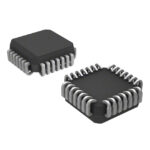 MC100E416FN

The activity of extra discounts on wholesale prices is in full swing…
Please fill in your contact information and we will send you the latest wholesale price list.







