 ChipApex | Global Electronic Components Supplier

SEARCH
Search Product
Search Post
— IC芯片 | 连接器 | 传感器 | 被动器件 —
Search productSearch post
— IC芯片 | 连接器 | 传感器 | 被动器件 —
Consult the customer manager about the wholesale price.
consultation hotline:86-132-6715-2157
email:[email protected]
Contact the product manager for consultation. One-stop consultation is available.
Do you want a lower wholesale price? Please send us your inquiry and we will reply immediately.
MC100EP142FAR2 is listed in the Shift Registers range at ChipApex. The manufacturer field lists onsemi. Its product description is IC REGISTER SHFT 9BIT ECL 32LQFP. Review the specifications below when checking this part for your BOM.
The MC100EP142FAR2G is a 9-bit shift register from the onsemi 100 Series, designed for byte-parity applications. It supports serial/parallel data input and serial/parallel output with unidirectional shifting capability. The device operates in PECL mode (VCC = 3.0 V to 5.5 V, VEE = 0 V) or NECL mode (VCC = 0 V, VEE = -3.0 V to -5.5 V). Key electrical parameters include a typical shift frequency exceeding 2.8 GHz, propagation delays of 500 ps to 800 ps depending on temperature, and setup times of 50 ps to 100 ps. It features asynchronous master reset, dual clock inputs (CLK0/CLK1), and internal input pull-down/pull-up resistors.
Verify the complete part number includes the 'R2G' suffix for tape and reel packaging and lead-free compliance. Confirm the specific logic family variant (MC10EP vs MC100EP) matches the required power supply configuration before ordering. Check current availability status as distribution may vary by region.
Select this component for designs requiring high-frequency ECL shifting with byte-wide data handling. Ensure the system power supply aligns with either PECL (+3.3V/+5V) or NECL (-3.3V/-5V) requirements. Verify thermal management needs, as airflow >500 lfpm is recommended for stable operation at higher voltages.
This device belongs to the MC10EP/MC100EP family of ECL logic devices manufactured by onsemi. The '100' prefix typically denotes compatibility with both 3.3V and 5V ECL standards, while the 'FAR2G' suffix indicates LQFP-32 packaging in a tape and reel format with RoHS compliance.
MC100EP142FAG is a compatible alternative in LQFP-32 tray packaging.
The SEL pin switches between SHIFT and LOAD modes. A LOW level enables LOAD mode where parallel inputs D0-D8 are captured, while a HIGH level enables SHIFT mode where data moves from Bit 0 to Bit 8 on the clock edge.
The Master Reset (MR) pin asynchronously resets all nine registers to zero when driven HIGH, overriding the CLK0 and CLK1 inputs regardless of their state.
Explore related parts through Logic, Integrated Circuits (ICs), all product categories, ChipApex homepage.
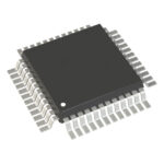 MC100EP142FAR2

The activity of extra discounts on wholesale prices is in full swing…
Please fill in your contact information and we will send you the latest wholesale price list.





