 ChipApex | Global Electronic Components Supplier

SEARCH
Search Product
Search Post
— IC芯片 | 连接器 | 传感器 | 被动器件 —
Search productSearch post
— IC芯片 | 连接器 | 传感器 | 被动器件 —
Consult the customer manager about the wholesale price.
consultation hotline:86-132-6715-2157
email:[email protected]
Contact the product manager for consultation. One-stop consultation is available.
Do you want a lower wholesale price? Please send us your inquiry and we will reply immediately.
MC100EP142MNG is listed in the Shift Registers range at ChipApex. The manufacturer field lists onsemi. Its product description is IC SHIFT REGISTER 9BIT ECL 32QFN. Review the specifications below when checking this part for your BOM.
The MC100EP142MNG is a 9-bit shift register from the onsemi 100EP series, designed for byte-parity applications. It operates in PECL mode with VCC ranging from 3.0 V to 5.5 V (VEE = 0 V) and NECL mode with VCC at 0 V and VEE from -3.0 V to -5.5 V. The device accepts serial or parallel data inputs and provides serial/parallel outputs, shifting directionally from Bit 0 to Bit 8. It features dual clock inputs (CLK0, CLK1), an asynchronous master reset, and supports shift frequencies exceeding 2.8 GHz. Packaged in a 32-lead QFN (5x5 mm) with an exposed pad.
Verify component authenticity through authorized distributors as this part number may be subject to obsolescence. Confirm package suffix 'MN' corresponds to the QFN-32 form factor. Check RoHS compliance status and moisture sensitivity level requirements during storage and handling. Ensure power supply decoupling meets ECL design guidelines for stable operation.
Select this component when byte-aligned parity operations are required within ECL logic families. Consider the QFN-32 package constraints regarding thermal dissipation and PCB layout. Verify compatibility with existing PECL or NECL power rails. Evaluate the need for dual-clock inputs versus single-clock alternatives based on system timing architecture.
Part of the MC100EP family utilizing temperature-compensated ECL technology. Designed for high-frequency digital applications requiring reliable data shifting and parity functions. Manufactured by onsemi using lead-free processes compliant with environmental standards.
MC100EP142FAG serves as a direct functional substitute offering identical electrical characteristics but housed in an LQFP-32 package instead of QFN-32. Verify pinout compatibility and thermal management requirements when transitioning between package types.
The SEL input switches between SHIFT and LOAD modes. When SEL is HIGH, the device shifts data on the positive clock edge. When SEL is LOW, parallel data inputs D0-D8 are loaded into the registers.
A HIGH signal on the MR pin asynchronously resets all nine registers to zero, immediately overriding the CLK0 and CLK1 inputs regardless of their current state.
Yes, to minimize power consumption, any Q output not utilized in the application should be left unterminated rather than connected to a load.
Explore related parts through Logic, Integrated Circuits (ICs), all product categories, ChipApex homepage.
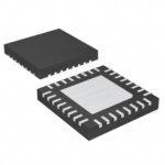 MC100EP142MNG

The activity of extra discounts on wholesale prices is in full swing…
Please fill in your contact information and we will send you the latest wholesale price list.





