 ChipApex | Global Electronic Components Supplier
SEARCH
Search Product
Search Post
— IC芯片 | 连接器 | 传感器 | 被动器件 —
Search productSearch post
— IC芯片 | 连接器 | 传感器 | 被动器件 —
Consult the customer manager about the wholesale price.
consultation hotline:86-132-6715-2157
email:[email protected]
Contact the product manager for consultation. One-stop consultation is available.
Do you want a lower wholesale price? Please send us your inquiry and we will reply immediately.
The MC100EP196BFAR2G is a 3.3 V ECL Programmable Delay Chip (PDC) designed for clock deskewing and timing adjustment. It provides variable delay of differential NECL/PECL input transitions with a digitally selectable resolution of approximately 10 ps and a net range up to 10.4 ns. The device features an FTUNE pin for analog fine-tuning of output delay from 0 to 60 ps. It operates within a supply voltage range of 3.0 V to 3.6 V in PECL mode or -3.0 V to -3.6 V in NECL mode, supporting maximum input clock frequencies exceeding 1.2 GHz.
Verify the specific suffix 'R2G' against official documentation to confirm reel packaging specifications and RoHS compliance status. Ensure that the ordering information matches the required package type and lead-free designation as defined by the manufacturer's current product release notes.
Select this component when precise sub-nanosecond delay adjustments are required for differential ECL signals. Consider the FTUNE pin requirement for analog control circuitry if finer resolution than 10 ps is needed. Verify power supply compatibility for either PECL (+3.3V) or NECL (-3.3V) operation modes before integration.
This device belongs to the MC100EP196B series, which includes variants like MC100EP196BMNG and MC100EP196BFAG. It shares architecture with the EP195 but adds FTUNE tunability. The BFAR2G suffix indicates a specific tape-and-reel packaging configuration for automated assembly, distinct from tube-packaged versions.
MC100EP196BMNG
The FTUNE pin accepts an analog voltage to provide fine-tuning of the output delay from 0 to 60 ps, supplementing the 10 ps digital resolution provided by the D inputs.
Due to the chain of multiplexers, the device has a fixed minimum delay of approximately 2.2 ns to 2.4 ns, regardless of the digital settings.
Yes, it supports cascading multiple PDCs using the D10 input and CASCADE outputs to increase the total programmable delay range beyond a single chip's limit.
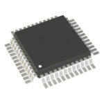 MC100EP196BFAR2G
The activity of extra discounts on wholesale prices is in full swing…
Please fill in your contact information and we will send you the latest wholesale price list.





