 ChipApex | Global Electronic Components Supplier

SEARCH
Search Product
Search Post
— IC芯片 | 连接器 | 传感器 | 被动器件 —
Search productSearch post
— IC芯片 | 连接器 | 传感器 | 被动器件 —
Consult the customer manager about the wholesale price.
consultation hotline:86-132-6715-2157
email:[email protected]
Contact the product manager for consultation. One-stop consultation is available.
Do you want a lower wholesale price? Please send us your inquiry and we will reply immediately.
MC100EP91DWR2G is listed in the Translators, Level Shifters range at ChipApex. The manufacturer field lists onsemi. Its product description is IC TRANSLATOR UNIDIR 20SOIC. Review the specifications below when checking this part for your BOM.
The MC100EP91DWR2G is a triple any-level positive input to NECL output translator manufactured by onsemi. It accepts LVPECL, LVTTL, LVCMOS, HSTL, CML, or LVDS signals and translates them to differential NECL outputs (-3.0 V/-5.5 V). The device operates with three power rails: VCC (2.375 V to 3.8 V), VEE (-3.0 V to -5.5 V), and GND (0 V). Key electrical parameters include a maximum input clock frequency exceeding 2.0 GHz typical, a maximum input data rate exceeding 2.0 Gb/s typical, and a typical propagation delay of 500 ps. It is housed in a SOIC-20 Wide Body package.
Verify the specific ordering suffix DWR2G corresponds to the SOIC-20 Wide Body package with tape and reel shipping configuration. Confirm RoHS compliance and lead-free status as indicated by the 'G' marking. Ensure design requirements align with the specified operating temperature range of -40°C to +85°C and the required three-power-rail supply architecture.
Select this component when interfacing positive voltage logic standards such as LVCMOS or LVPECL with NECL-compatible downstream devices. The device supports up to three independent channels within a single package. Designers must account for the requirement of separate positive and negative supply rails and ensure proper decoupling of VCC and VEE pins with 0.01 µF capacitors to ground.
This part belongs to the MC100EP91 series of translators from onsemi. The DWR2G suffix specifically denotes the SOIC-20 Wide Body package variant supplied in a 1000-unit tape and reel format. Other variants in the family include tube-packaged versions like the DWG and the discontinued MN suffix QFN-24 package.
The NB100LVEP91DWG is listed as a manufacturer-recommended alternative for the MC100EP91DWG. Verify pinout compatibility and electrical specifications before substituting, as package and performance characteristics may differ between the EP91 and LVEP91 series.
Under open input conditions, the D input is biased at VCC/2 and the D-bar input is pulled to GND. This forces the Q outputs to a low state and the Q-bar outputs to a high state, ensuring system stability.
The VBB pin provides an internally generated PECL reference voltage. It can be used as a switching reference for single-ended inputs or to rebias AC-coupled inputs. When used, it must be decoupled via a 0.01 µF capacitor.
Explore related parts through Logic, Integrated Circuits (ICs), all product categories, ChipApex homepage.
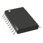 MC100EP91DWR2G

The activity of extra discounts on wholesale prices is in full swing…
Please fill in your contact information and we will send you the latest wholesale price list.






