 ChipApex | Global Electronic Components Supplier

SEARCH
Search Product
Search Post
— IC芯片 | 连接器 | 传感器 | 被动器件 —
Search productSearch post
— IC芯片 | 连接器 | 传感器 | 被动器件 —
Consult the customer manager about the wholesale price.
consultation hotline:86-132-6715-2157
email:[email protected]
Contact the product manager for consultation. One-stop consultation is available.
Do you want a lower wholesale price? Please send us your inquiry and we will reply immediately.
MC100EPT21D is listed in the Translators, Level Shifters range at ChipApex. The manufacturer field lists onsemi. Its product description is IC XLATOR LVPECL-LVTTL DFF 8SOIC. Review the specifications below when checking this part for your BOM.
The MC100EPT21 is a differential LVPECL/LVDS/CML to LVTTL/LVCMOS translator designed for clock or data signal translation. It operates on a single +3.3 V supply with ground, eliminating the need for negative voltages. The device features a typical propagation delay of 1.4 ns and supports maximum frequencies exceeding 275 MHz. It includes an internal VBB output reference voltage for AC-coupled inputs in both single-ended and differential modes. The component is available in SOIC-8, TSSOP-8, and DFN8 packages.
Verify package suffix compatibility (DG for SOIC-8, DTG for TSSOP-8, MNR4G for DFN8) against board layout requirements. Confirm RoHS compliance status and Pb-free marking presence during inspection. Ensure thermal management strategies align with junction-to-ambient resistance values specified for the selected package type under standard airflow conditions.
Select this component when translating from differential ECL-family standards to standard CMOS/TTL logic without requiring negative supply rails. Consider the specific package thermal characteristics if operating near maximum temperature limits. Evaluate input coupling methods; direct connection requires external biasing, while AC coupling utilizes the internal VBB pin.
Part of the MC100EPT2 series, which provides differential translation capabilities. The 100 Series designation indicates temperature compensation features inherent to onsemi's ECL family products. This specific model focuses on converting positive ECL variants and related standards to lower voltage digital logic families.
Check datasheet for functional equivalents within the same family. Verify pinout compatibility and electrical specifications match before substitution. No specific substitute part numbers are confirmed in the provided documentation.
For single-ended AC coupling, tie the VBB output to the D input. For differential AC coupling, connect the VBB output through a resistor to each input pin. Bypass the VBB pin to VCC via a 0.01 µF capacitor if used.
If left open, the D input pulls down to VEE and the D_bar input biases around VCC/2. The outputs will go to a defined state, though the specific state depends on the power-up sequence.
Explore related parts through Logic, Integrated Circuits (ICs), all product categories, ChipApex homepage.
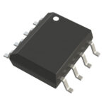 MC100EPT21D

The activity of extra discounts on wholesale prices is in full swing…
Please fill in your contact information and we will send you the latest wholesale price list.







