 ChipApex | Global Electronic Components Supplier

SEARCH
Search Product
Search Post
— IC芯片 | 连接器 | 传感器 | 被动器件 —
Search productSearch post
— IC芯片 | 连接器 | 传感器 | 被动器件 —
Consult the customer manager about the wholesale price.
consultation hotline:86-132-6715-2157
email:[email protected]
Contact the product manager for consultation. One-stop consultation is available.
Do you want a lower wholesale price? Please send us your inquiry and we will reply immediately.
MC100ES6011EJR2 is listed in the Clock Buffers, Drivers range at ChipApex. The manufacturer field lists Renesas Electronics Corporation. Its product description is IC CLK BUFFER 1:2 3GHZ 8TSSOP. Review the specifications below when checking this part for your BOM.
The MC100ES6011EJR2 is a differential 1:2 fanout buffer from the 100ES series, designed for applications requiring lower voltage operation. It supports PECL mode with VCC ranging from 2.375 V to 3.8 V (VEE = 0 V) and ECL mode with VEE from -2.375 V to -3.8 V (VCC = 0 V). The device features a typical propagation delay of 270 ps and operates at maximum frequencies exceeding 3 GHz. It includes temperature compensation and LVDS input compatibility. The component is housed in an 8-lead TSSOP package.
This component has been discontinued by the manufacturer. The last time buy expired on December 19, 2013. Current availability is limited to existing stock or surplus channels. Verification of authenticity and storage conditions is critical due to the age of available units and potential moisture sensitivity issues.
Select this part for designs requiring a differential 1:2 fanout buffer with high-speed performance up to 3 GHz. Ensure the power supply configuration matches either PECL or ECL requirements. Note that the device defaults outputs LOW when inputs are open. Verify thermal resistance requirements, as junction-to-ambient resistance varies based on airflow conditions.
The MC100ES6011 belongs to the 100ES series, which incorporates temperature compensation for stable performance across varying environmental conditions. Originally manufactured by Integrated Device Technology, Inc., the product line was later acquired by Renesas Electronics Corporation. The 'EJ' suffix specifically denotes the Pb-Free 8-lead TSSOP package variant.
As the MC100ES6011 is discontinued, direct replacements must be sourced from current inventory or alternative suppliers. No official cross-reference part numbers are provided in the datasheet. Designers should evaluate other differential fanout buffers from the same family or newer generations that maintain similar pinouts and electrical specifications.
When the inputs are left open or at VEE, the Q output will default LOW.
Yes, the device is LVDS input compatible.
The maximum frequency is typically greater than 3 GHz.
Explore related parts through Clock/Timing, Integrated Circuits (ICs), all product categories, ChipApex homepage.
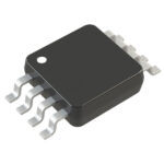 MC100ES6011EJR2

The activity of extra discounts on wholesale prices is in full swing…
Please fill in your contact information and we will send you the latest wholesale price list.





