 ChipApex | Global Electronic Components Supplier

SEARCH
Search Product
Search Post
— IC芯片 | 连接器 | 传感器 | 被动器件 —
Search productSearch post
— IC芯片 | 连接器 | 传感器 | 被动器件 —
Consult the customer manager about the wholesale price.
consultation hotline:86-132-6715-2157
email:[email protected]
Contact the product manager for consultation. One-stop consultation is available.
Do you want a lower wholesale price? Please send us your inquiry and we will reply immediately.
MC100LVEL39DWR2 is listed in the Clock Generators, PLLs, Frequency Synthesizers range at ChipApex. The manufacturer field lists onsemi. Its product description is IC CLOCK GEN ECL 2:4 4/6 20SOIC. Review the specifications below when checking this part for your BOM.
The MC100LVEL39DWR2 is a low skew clock generation chip designed for precise timing applications. It provides ÷2/4 and ÷4/6 division ratios with internal dividers synchronous to each other, ensuring aligned output edges. The device accepts differential or single-ended inputs and supports PECL (VCC = 3.0 V to 3.8 V) and NECL (VEE = −3.0 V to −3.8 V) modes. Key electrical parameters include a maximum toggle frequency of 1000 MHz, 50 ps maximum output-to-output skew, and propagation delays ranging from 600 ps to 1250 ps depending on the path. It features synchronous enable/disable and master reset capabilities.
Verify RoHS compliance and Pb-Free status as indicated by the 'G' suffix in ordering information. Confirm package type SOIC-20 WB and shipping quantity (1000/Tape & Reel). Check moisture sensitivity level (Level 3) requirements for storage and handling. Ensure power supply connections for all VCC and VEE pins are externally connected for proper operation.
Select this component when precise phase alignment between multiple divided clocks is required. The synchronous divider design ensures common output edges are aligned. Consider the 1000 MHz maximum toggle frequency and 50 ps skew limits for high-speed applications. Verify compatibility with existing PECL or NECL logic families and ensure appropriate termination networks are used.
Part of the MC100LVEL series, which contains temperature-compensated devices. The MC100LVEL39 specifically addresses clock generation needs with dual division ratios. It is manufactured by onsemi (formerly Motorola/NXP logic line). The device integrates 419 transistors and meets JEDEC latchup test specifications.
MC100LVEL39DWR2G is the Pb-Free variant of the MC100LVEL39DWR2. No direct cross-manufacturer substitutes are listed in the provided documentation. Verify pinout and electrical characteristics if considering alternative low-skew clock generators.
For single-ended input conditions, the unused differential input is connected to the VBB pin, which serves as a switching reference voltage. VBB can also rebias AC coupled inputs.
The Master Reset input ensures synchronization across systems utilizing multiple LVEL39 chips. Upon startup, internal flip-flops attain a random state; asserting MR aligns them. For single-device systems, MR is not strictly necessary due to internal divider synchronization.
Yes, by using the VBB output, a sinusoidal source can be AC coupled into the device. The VBB pin provides an internally generated reference voltage suitable for this purpose.
Explore related parts through Clock/Timing, Integrated Circuits (ICs), all product categories, ChipApex homepage.
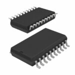 MC100LVEL39DWR2

The activity of extra discounts on wholesale prices is in full swing…
Please fill in your contact information and we will send you the latest wholesale price list.







