 ChipApex | Global Electronic Components Supplier

SEARCH
Search Product
Search Post
— IC芯片 | 连接器 | 传感器 | 被动器件 —
Search productSearch post
— IC芯片 | 连接器 | 传感器 | 被动器件 —
Consult the customer manager about the wholesale price.
consultation hotline:86-132-6715-2157
email:[email protected]
Contact the product manager for consultation. One-stop consultation is available.
Do you want a lower wholesale price? Please send us your inquiry and we will reply immediately.
MC100LVEP11MNR4 is listed in the Clock Buffers, Drivers range at ChipApex. The manufacturer field lists onsemi. Its product description is IC CLK BUFFER 1:2 3GHZ 8DFN. Review the specifications below when checking this part for your BOM.
The MC100LVEP11MNR4G is a differential 1:2 fanout buffer from the 100 Series, featuring temperature compensation. It operates in PECL mode with VCC ranging from 2.375 V to 3.8 V (VEE = 0 V) or NECL mode with VEE from −3.8 V to −2.375 V (VCC = 0 V). The device supports a maximum frequency exceeding 3.0 GHz and exhibits a typical propagation delay of 240 ps. It provides two complementary outputs per input pair, ensuring low output-to-output skew of less than 20 ps. The component is housed in an 8-lead DFN package.
Verify the complete ordering code includes the 'G' suffix for RoHS compliance and Pb-Free status. Confirm the 'MN' suffix corresponds to the DFN-8 package variant. Ensure the datasheet revision matches the required specifications for your design implementation.
Select the MC100LVEP11 variant when temperature compensation is required, as opposed to the MC10LVEP11. Choose the DFN-8 package for space-constrained designs requiring thermal exposure pad connection. Verify power supply constraints align with the specified PECL or NECL operating ranges.
This component belongs to the MC10/100LVEP11 family, which are pin and functionally equivalent to the EP11 device. The 100 Series specifically includes internal temperature compensation circuitry to maintain performance stability across the industrial temperature range of -40°C to +85°C.
Public confirmed substitute part numbers are not available in the provided documentation.
Explore related parts through Clock/Timing, Integrated Circuits (ICs), all product categories, ChipApex homepage.
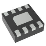 MC100LVEP11MNR4

The activity of extra discounts on wholesale prices is in full swing…
Please fill in your contact information and we will send you the latest wholesale price list.




