 ChipApex | Global Electronic Components Supplier
SEARCH
Search Product
Search Post
— IC芯片 | 连接器 | 传感器 | 被动器件 —
Search productSearch post
— IC芯片 | 连接器 | 传感器 | 被动器件 —
Consult the customer manager about the wholesale price.
consultation hotline:86-132-6715-2157
email:[email protected]
Contact the product manager for consultation. One-stop consultation is available.
Do you want a lower wholesale price? Please send us your inquiry and we will reply immediately.
The MC10E196FNR2 is a programmable delay chip (PDC) designed for accurate differential ECL input edge placement. It features a chain of gates and a linear ramp delay adjustment, providing a worst-case delay range of 2.0 ns with approximately 20 ps per step resolution. The device includes an FTUNE analog input to further reduce the minimum LSB resolution. It operates in PECL mode with VCC from 4.2 V to 5.7 V (VEE = 0 V) or NECL mode with VEE from -4.2 V to -5.7 V (VCC = 0 V). The component has a bandwidth greater than 1.0 GHz and contains on-chip cascade circuitry for extended programmable ranges.
Verify the specific ordering suffix to confirm package type and shipping quantity. The FNR2 suffix indicates a PLCC-28 package supplied in tape and reel format containing 500 units. Confirm RoHS compliance status if required by the design specifications, noting that Pb-Free variants carry an additional G suffix.
Select this component when precise programmable delay is required for high-speed ECL signals. Ensure the design supports either PECL or NECL power supply configurations. Consider using the FTUNE pin with an external DAC if sub-20 ps resolution is necessary. Verify that the system can accommodate the required thermal management for the PLCC-28 package.
This part belongs to the MC10E/100E196 series of programmable delay chips manufactured by onsemi. It is functionally similar to the MC10E195 but adds the FTUNE analog input for finer resolution. The 100 Series variant includes temperature compensation, whereas the 10 Series does not. Both share the same pinout and core functionality.
The MC10E195 serves as a related model within the same family but lacks the FTUNE analog input feature. When replacing the MC10E196FNR2 with the MC10E195, verify that the application does not require the enhanced resolution provided by the linear ramp delay adjustment.
The FTUNE pin accepts an analog voltage that applies a linear ramp to the internal delay circuitry. This allows for delay adjustments finer than the 20 ps digital resolution provided by the address inputs, effectively reducing the minimum LSB step size.
The VBB pin provides an internally generated reference voltage. It can be used as a switching reference voltage for single-ended input conditions by connecting the unused differential input to it, or to rebias AC coupled inputs.
Multiple devices are cascaded using the D7 input and the CASCADE outputs. Asserting D7 on the first chip signals the need for additional delay range, which controls the SET MIN pin of the subsequent chip. This allows chaining without external gating, adding only one address line per device.
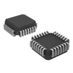 MC10E196FNR2
The activity of extra discounts on wholesale prices is in full swing…
Please fill in your contact information and we will send you the latest wholesale price list.





