 ChipApex | Global Electronic Components Supplier

SEARCH
Search Product
Search Post
— IC芯片 | 连接器 | 传感器 | 被动器件 —
Search productSearch post
— IC芯片 | 连接器 | 传感器 | 被动器件 —
Consult the customer manager about the wholesale price.
consultation hotline:86-132-6715-2157
email:[email protected]
Contact the product manager for consultation. One-stop consultation is available.
Do you want a lower wholesale price? Please send us your inquiry and we will reply immediately.
MC10EP35DG is listed in the Flip Flops range at ChipApex. The manufacturer field lists onsemi. Its product description is IC FF JK TYPE SNGL 1BIT 8SOIC. Review the specifications below when checking this part for your BOM.
The MC10EP35DG is a single JK flip-flop from the onsemi 10EP series, designed for high-speed ECL applications. It features differential outputs and positive-edge triggering within an 8-SOIC surface-mount package. The device supports PECL operation with VCC ranging from 3.0 V to 5.5 V and NECL operation with VEE from -3.0 V to -5.5 V. It includes an asynchronous reset function and operates across a temperature range of -40°C to +85°C.
Verify that the specific procurement channel provides the 8-SOIC tube packaging indicated in the product parameters. Confirm that the supply voltage rails match the required PECL or NECL configuration before integration. Ensure thermal management aligns with the specified -40°C to +85°C operating range for the target environment.
Select this component when a single JK flip-flop with differential outputs is required for speeds up to 3 GHz. Compare against the MC10EP35D variant if lead-free compliance is not a primary constraint, as the DG suffix typically denotes RoHS-compliant packaging. Ensure the design accommodates the 50 mA quiescent current draw typical of the 10EP series.
This part belongs to the MC10/100EP series, which represents a higher-speed, low-voltage evolution of the earlier EL35 JK flip-flop. The 10EP family is optimized for performance in PECL and NECL environments, offering faster propagation delays compared to legacy ECL counterparts while maintaining compatibility with standard ECL power supplies.
Direct replacements include the MC10EP35D for non-RoHS applications or the MC10EL35 for legacy designs. When substituting, verify pinout compatibility and ensure the new component supports the required differential output swing and power supply voltage ranges.
In PECL mode, VCC is set between 3.0 V and 5.5 V with VEE at 0 V. In NECL mode, VCC is at 0 V and VEE is set between -3.0 V and -5.5 V.
The device has an open-input default state where the Q output will default LOW if inputs are open or connected to VEE.
The reset pin is asynchronous and is activated by a logic HIGH signal, independent of the clock edge.
Explore related parts through Logic, Integrated Circuits (ICs), all product categories, ChipApex homepage.
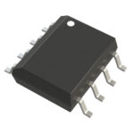 MC10EP35DG

The activity of extra discounts on wholesale prices is in full swing…
Please fill in your contact information and we will send you the latest wholesale price list.






