 ChipApex | Global Electronic Components Supplier

SEARCH
Search Product
Search Post
— IC芯片 | 连接器 | 传感器 | 被动器件 —
Search productSearch post
— IC芯片 | 连接器 | 传感器 | 被动器件 —
Consult the customer manager about the wholesale price.
consultation hotline:86-132-6715-2157
email:[email protected]
Contact the product manager for consultation. One-stop consultation is available.
Do you want a lower wholesale price? Please send us your inquiry and we will reply immediately.
MC10EP51MNTAG is listed in the Flip Flops range at ChipApex. The manufacturer field lists onsemi. Its product description is IC FF D-TYPE SNGL 1BIT 8DFN. Review the specifications below when checking this part for your BOM.
The MC10EP51MNTAG is a high-speed ECL D flip-flop with reset and differential clock inputs, part of the MC10EP51 series. It operates on a single supply voltage ranging from 3 V to 5.5 V. The device features an exposed pad for thermal management and is housed in an 8-lead VFDFN package measuring 4x4 mm with a height of 1.5 mm. It supports positive or negative edge triggering via configurable differential clock inputs. The component ensures stable operation with internal clamping circuits for floating inputs and offers typical propagation delays around 320 ps at 3.3 V PECL mode.
Verify the specific ordering suffix 'MNTAG' corresponds to the required tape and reel packaging quantity and RoHS compliance status. Confirm that the 8-VFDFN package variant matches the PCB footprint requirements. Ensure the selected revision aligns with the intended operating temperature range and electrical specifications for the target application environment.
Select this component for designs demanding low jitter and precise phase alignment in synchronous digital systems. The differential clock architecture minimizes common-mode noise susceptibility compared to single-ended alternatives. Consider the exposed pad requirement for adequate thermal grounding during high-frequency operation to maintain signal integrity and device reliability.
This device belongs to the MC10EP51 series of ECLinPS logic family components. It serves as a direct pin-compatible upgrade to earlier EL51 and LVEL51 models. The series provides high-performance data storage elements optimized for modern high-speed serial communication interfaces and clock recovery circuits.
MC10EP51DTG
The differential clock input can be configured to trigger on either the positive or negative edge, eliminating the need for external inverters and reducing path delay.
Internal clamping circuits pull the non-inverted clock (CLK) to VEE and bias the inverted clock (CLK#) to VCC/2, preventing indeterminate output states.
Explore related parts through Logic, Integrated Circuits (ICs), all product categories, ChipApex homepage.
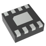 MC10EP51MNTAG

The activity of extra discounts on wholesale prices is in full swing…
Please fill in your contact information and we will send you the latest wholesale price list.






