 ChipApex | Global Electronic Components Supplier
SEARCH
Search Product
Search Post
— IC芯片 | 连接器 | 传感器 | 被动器件 —
Search productSearch post
— IC芯片 | 连接器 | 传感器 | 被动器件 —
Consult the customer manager about the wholesale price.
consultation hotline:86-132-6715-2157
email:[email protected]
Contact the product manager for consultation. One-stop consultation is available.
Do you want a lower wholesale price? Please send us your inquiry and we will reply immediately.
The MC10H640FNG is a clock driver designed for 68030 and 68040 microprocessors. It accepts TTL or PECL inputs and provides six TTL outputs with internal divide-by-two and divide-by-four stages. The device operates on a single +5.0 V supply (4.75 V to 5.25 V) and supports maximum input frequencies up to 135 MHz. Propagation delay ranges from 4.0 ns to 6.3 ns depending on the output stage, with within-device skew limited to 0.5 ns. It features an asynchronous reset function and is housed in a 28-lead PLCC package.
Verify component authenticity through authorized channels as counterfeit risks exist for legacy logic ICs. Confirm RoHS compliance status and moisture sensitivity level (MSL 3) prior to surface mount assembly. Check for specific ordering suffixes if tube packaging is required instead of standard bulk options.
Select this component when interfacing differential ECL/PECL signals to TTL loads for 68030/040 MPU architectures. Ensure load capacitance remains within specified limits (e.g., 10 pF to 50 pF) to maintain duty cycle accuracy at high frequencies. Verify that the 28-PLCC footprint matches the target PCB layout constraints.
This device belongs to the MC10H series of high-speed ECL/TTL logic components manufactured by onsemi. It is specifically engineered to meet the strict timing requirements of older 32-bit microprocessor families. The FNG suffix indicates a lead-free, halogen-free PLCC-28 package compliant with RoHS directives.
Direct pin-compatible replacements are not explicitly listed in the provided documentation. Evaluate other devices within the MC10H64x family or general-purpose clock drivers that support PECL/TTL translation and match the 28-PLCC form factor.
The H640 includes circuitry to force a stable state if both sides of the ECL input differential pair are left open. In this scenario, the DE side is pulled LOW and DE_bar goes HIGH.
The maximum input frequency is 135 MHz under standard test conditions with a 25 pF load capacitance.
The device is designed so that the positive edges of the ÷2 and ÷4 outputs are synchronized at power up.
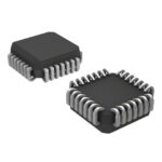 MC10H640FNG
The activity of extra discounts on wholesale prices is in full swing…
Please fill in your contact information and we will send you the latest wholesale price list.






