 ChipApex | Global Electronic Components Supplier

SEARCH
Search Product
Search Post
— IC芯片 | 连接器 | 传感器 | 被动器件 —
Search productSearch post
— IC芯片 | 连接器 | 传感器 | 被动器件 —
Consult the customer manager about the wholesale price.
consultation hotline:86-132-6715-2157
email:[email protected]
Contact the product manager for consultation. One-stop consultation is available.
Do you want a lower wholesale price? Please send us your inquiry and we will reply immediately.
MC10H641FNR2G is listed in the Clock Buffers, Drivers range at ChipApex. The manufacturer field lists onsemi. Its product description is IC CLK BUFFER 1:9 65MHZ 28PLCC. Review the specifications below when checking this part for your BOM.
The MC10H641FNR2G is a single-supply, low-skew translating 1:9 clock driver manufactured by onsemi. It converts PECL inputs to TTL outputs within a PLCC-28 package. The device operates on a single +5.0 V supply with separate ECL and TTL power pins. Key electrical parameters include a maximum input frequency of 65 MHz at 50 pF load, propagation delays ranging from 4.86 ns to 6.43 ns depending on temperature, and output drive capabilities of 24 mA. It features differential ECL internal design, logic enable, latch enable, and a VBB reference output for single-ended use.
Verify the 'G' suffix indicates a Pb-Free package compliant with RoHS standards. Confirm the 'R2' suffix corresponds to Tape & Reel packaging containing 500 units per reel. Ensure the specific revision (Rev.7) matches the required documentation version for design-in validation.
Select this component when a 1:9 split ratio between PECL source and TTL destinations is required. Evaluate thermal resistance and airflow conditions to determine junction temperature, as AC characteristics are specified based on junction temperature rather than ambient temperature. Ensure load capacitance does not exceed 50 pF for guaranteed timing parameters.
This part belongs to the H641 translator series designed for optimal power pinning and signal flow. It serves as the PECL-TTL variant of the popular ECLinPS family. The device utilizes the PLCC-28 package (Case 776) to support separate power supplies for ECL and TTL sections, minimizing noise coupling between logic domains.
The MC100H641FNR2G is functionally equivalent but compatible with positive 100K logic levels instead of MECL 10H levels. Both share identical pinouts and electrical characteristics regarding the TTL output stage and skew performance.
The VBB pin provides a positive ECL reference voltage output. For single-ended input applications, it should be connected to the D input and bypassed with a 0.01 µF capacitor.
Propagation delay varies with junction temperature, supply voltage (VCC), and capacitive load. The datasheet specifies limits based on junction temperature, requiring calculation of thermal resistance and power dissipation for precise skew estimation.
LEN (Latch Enable) controls the transparency of the input latch; when LOW, the latch is transparent. EN (Enable) forces all outputs LOW when HIGH. Both are positive ECL inputs.
Explore related parts through Clock/Timing, Integrated Circuits (ICs), all product categories, ChipApex homepage.
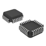 MC10H641FNR2G

The activity of extra discounts on wholesale prices is in full swing…
Please fill in your contact information and we will send you the latest wholesale price list.





