 ChipApex | Global Electronic Components Supplier

SEARCH
Search Product
Search Post
— IC芯片 | 连接器 | 传感器 | 被动器件 —
Search productSearch post
— IC芯片 | 连接器 | 传感器 | 被动器件 —
Consult the customer manager about the wholesale price.
consultation hotline:86-132-6715-2157
email:[email protected]
Contact the product manager for consultation. One-stop consultation is available.
Do you want a lower wholesale price? Please send us your inquiry and we will reply immediately.
MC10LVEP16DR2 is listed in the Specialty Logic range at ChipApex. The manufacturer field lists onsemi. Its product description is IC RECEIVER/DRVR DIFF ECL 8-SOIC. Review the specifications below when checking this part for your BOM.
The MC10LVEP16DR2 is a differential receiver/driver from the MC10/100LVEP16 series by onsemi. It operates in PECL mode with VCC ranging from 2.375 V to 3.8 V (VEE = 0 V) and NECL mode with VEE ranging from -2.375 V to -3.8 V (VCC = 0 V). The device features a typical propagation delay of 240 ps and supports maximum frequencies exceeding 4 GHz. It includes an internally generated VBB reference voltage output, open input default states, and LVDS input compatibility.
Verify the specific suffix 'DR2' against the official ordering information table to confirm package type and shipping format. Check current product status as some variants in this family are discontinued. Ensure compliance with RoHS and Pb-Free requirements if applicable to the specific revision. Confirm thermal management needs based on the selected package's thermal resistance ratings.
Select this component for applications requiring world-class differential receiver/driver performance with fast transition times. Consider the MC100 series variant if temperature compensation is required. Verify that the operating voltage range aligns with the system's PECL or NECL configuration. Ensure proper decoupling of the VBB pin if utilized for single-ended inputs or AC coupling biasing.
The MC10LVEP16 belongs to the MC10/100LVEP16 family of ECL differential receiver/drivers. This family is designed for high-speed data transmission and signal processing. The device is functionally comparable to other industry-standard ECL logic devices but offers enhanced speed characteristics suitable for demanding high-frequency interfaces.
MC10EP16DTR2G
The VBB pin provides an internally generated voltage supply. It can be used as a switching reference voltage for unused differential inputs in single-ended conditions or to rebias AC coupled inputs. It must be decoupled via a 0.01 µF capacitor when used.
When left open, the D pins will default to a LOW state due to internal pulldown resistors, while the D* pins will default to VCC/2 due to internal pullup resistors.
Yes, the device features LVDS input compatibility, allowing it to interface with LVDS sources.
Explore related parts through Logic, Integrated Circuits (ICs), all product categories, ChipApex homepage.
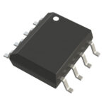 MC10LVEP16DR2

The activity of extra discounts on wholesale prices is in full swing…
Please fill in your contact information and we will send you the latest wholesale price list.







