 ChipApex | Global Electronic Components Supplier

SEARCH
Search Product
Search Post
— IC芯片 | 连接器 | 传感器 | 被动器件 —
Search productSearch post
— IC芯片 | 连接器 | 传感器 | 被动器件 —
Consult the customer manager about the wholesale price.
consultation hotline:86-132-6715-2157
email:[email protected]
Contact the product manager for consultation. One-stop consultation is available.
Do you want a lower wholesale price? Please send us your inquiry and we will reply immediately.
MC14007UBCPG is listed in the Specialty Logic range at ChipApex. The manufacturer field lists onsemi. Its product description is IC INVERTER DUAL COMP 14DIP. Review the specifications below when checking this part for your BOM.
The MC14007UB is a multipurpose device containing three N-Channel and three P-Channel enhancement mode MOSFETs with an additional inverter. It operates within a supply voltage range of 3.0 Vdc to 18 Vdc. The package provides individual access to each transistor's gate, drain, and source terminals. Input protection diodes are integrated on all inputs. The device supports driving low-power TTL loads and features pin-for-pin compatibility with CD4007A or CD4007UB equivalents.
Verify the specific ordering suffix to confirm package type and tape/reel specifications. Confirm if the NLV prefix is required for automotive applications necessitating unique site control and PPAP capability. Ensure compliance with RoHS standards and lead-free requirements during procurement. Check datasheet revisions for any updates to maximum ratings or electrical characteristics before finalizing orders.
Select this component when discrete access to multiple MOSFET terminals is required for custom analog or digital designs. Consider the wide supply voltage range for flexible power rail integration. Evaluate the drive current capabilities against load requirements. Verify thermal dissipation limits relative to ambient temperature conditions. Choose the NLV prefix variant only if automotive qualification and specific manufacturing controls are mandated by the system design.
This part belongs to the MC14007 series of multipurpose CMOS devices. It serves as a foundational building block for creating custom logic functions and analog switches using discrete MOSFET structures. The device complements standard logic gates by providing raw transistor elements accessible via a single package, facilitating compact implementations of complex switching topologies.
Pin-for-pin replacement is confirmed for CD4007A and CD4007UB devices. Verify electrical parameter tolerances match application requirements when substituting these legacy equivalents. Ensure that the replacement device meets the same operating voltage and temperature ranges specified in the original design constraints.
The substrates of the P-Channel devices are internally connected to VDD, while the substrates of the N-Channel devices are internally connected to VSS.
The device has two outputs without ESD protection; antistatic precautions must be taken when handling these specific pins.
Yes, it is capable of driving two low-power TTL loads or one low-power Schottky TTL load over the rated temperature range.
Explore related parts through Logic, Integrated Circuits (ICs), all product categories, ChipApex homepage.
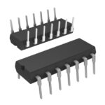 MC14007UBCPG

The activity of extra discounts on wholesale prices is in full swing…
Please fill in your contact information and we will send you the latest wholesale price list.





