 ChipApex | Global Electronic Components Supplier

SEARCH
Search Product
Search Post
— IC芯片 | 连接器 | 传感器 | 被动器件 —
Search productSearch post
— IC芯片 | 连接器 | 传感器 | 被动器件 —
Consult the customer manager about the wholesale price.
consultation hotline:86-132-6715-2157
email:[email protected]
Contact the product manager for consultation. One-stop consultation is available.
Do you want a lower wholesale price? Please send us your inquiry and we will reply immediately.
MC14053BDR2 is listed in the Analog Switches, Multiplexers, Demultiplexers range at ChipApex. The manufacturer field lists onsemi. Its product description is IC MUX/DEMUX TRIPLE 2X1 16SOIC. Review the specifications below when checking this part for your BOM.
The MC14053BDR2 is a digitally controlled analog switch implementing three independent SPDT (Single Pole Double Throw) switches. It operates on a single supply voltage ranging from 3.0 Vdc to 18 Vdc, with the analog signal range spanning the full supply difference between VDD and VEE. The device features low ON impedance and very low OFF leakage current, ensuring efficient signal routing. Control inputs are referenced to VSS, while analog I/O channels reference VEE. The component includes triple diode protection on control inputs and utilizes a break-before-make switching function to prevent signal overlap during channel transitions.
Verify the specific ordering suffix against the manufacturer's official documentation to confirm package type and tape/reel specifications. Ensure the procurement source provides valid RoHS compliance declarations and Pb-Free status certificates as specified in the datasheet. Cross-reference the part number with authorized distributors to confirm authenticity and traceability requirements for the intended application environment.
Select this component when a Triple SPDT configuration is required within the standard 4000 series CMOS logic family. Verify that the operating voltage range of 3.0 V to 18 V aligns with the system power rails. Consider the propagation delay characteristics if high-speed signal switching is critical, and ensure that the control logic levels are compatible with the VDD and VSS supply voltages provided in the design.
This device belongs to the MC14051B, MC14052B, and MC14053B series of analog multiplexers manufactured by onsemi. It serves as a pin-for-pin replacement for legacy CD4053 devices. The series is designed for general-purpose analog signal switching applications requiring low noise and linearized transfer characteristics across a wide supply voltage range.
MC14053BDG
While the absolute maximum rating allows up to 18.0 V, the datasheet recommends a maximum difference of 15 V between VDD and VEE for optimal parameter specification.
Control inputs (INH, A, B, C) are referenced to VSS, whereas the analog input/output channels (X, Y, Z) are referenced to VEE.
The device employs a 'break before make' switching function, ensuring that the previous connection is断开 before the new connection is established.
Explore related parts through Interface, Integrated Circuits (ICs), all product categories, ChipApex homepage.
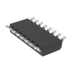 MC14053BDR2

The activity of extra discounts on wholesale prices is in full swing…
Please fill in your contact information and we will send you the latest wholesale price list.





