 ChipApex | Global Electronic Components Supplier

SEARCH
Search Product
Search Post
— IC芯片 | 连接器 | 传感器 | 被动器件 —
Search productSearch post
— IC芯片 | 连接器 | 传感器 | 被动器件 —
Consult the customer manager about the wholesale price.
consultation hotline:86-132-6715-2157
email:[email protected]
Contact the product manager for consultation. One-stop consultation is available.
Do you want a lower wholesale price? Please send us your inquiry and we will reply immediately.
MC14066BD is listed in the Analog Switches, Multiplexers, Demultiplexers range at ChipApex. The manufacturer field lists onsemi. Its product description is IC MULTIPLEXER QUAD 4X1 14SOIC. Review the specifications below when checking this part for your BOM.
The MC14066BD is a quad analog switch manufactured by onsemi, housed in a SOIC-14 package. It operates within a supply voltage range of 3.0 Vdc to 18.0 Vdc and supports an ambient temperature range from -55°C to +125°C. The device features four independent bilateral switches with a maximum ON resistance of 280 ohms at 15 V supply. Propagation delays are specified up to 120 ns, while the off-channel leakage current reaches 1000 nA at 125°C. Input capacitance is typically 5.0 pF, and the package power dissipation is rated at 500 mW.
Verify the specific suffix 'D' corresponds to the SOIC-14 package style when sourcing. Confirm RoHS compliance status as manufacturing revisions may affect material declarations. Check for discontinued status notifications from onsemi prior to finalizing procurement plans.
Select this component for designs requiring low noise performance with typical values around 12 nV/sqrt(Cycle). Ensure input signals remain within the VSS to VDD range to prevent latch-up. Consider the HC4066 if lower ON resistance is required for high-speed applications.
This part belongs to the MC14066B series of quad analog switches. It serves as a direct replacement for older Motorola and standard CMOS equivalents like the CD4016. The device is designed for general-purpose analog signal routing in mixed-signal environments.
While the absolute maximum rating is 18 V, the datasheet recommends a maximum difference of 15 V between VDD and VSS for optimal parameter specification.
Unused inputs must always be tied to an appropriate logic voltage level, either VSS or VDD. Unused outputs should be left open.
Standard parts are not explicitly qualified for automotive use. However, the NLV prefix variants are AEC-Q100 qualified and PPAP capable for such requirements.
Explore related parts through Interface, Integrated Circuits (ICs), all product categories, ChipApex homepage.
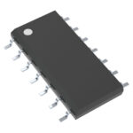 MC14066BD

The activity of extra discounts on wholesale prices is in full swing…
Please fill in your contact information and we will send you the latest wholesale price list.





