 ChipApex | Global Electronic Components Supplier

SEARCH
Search Product
Search Post
— IC芯片 | 连接器 | 传感器 | 被动器件 —
Search productSearch post
— IC芯片 | 连接器 | 传感器 | 被动器件 —
Consult the customer manager about the wholesale price.
consultation hotline:86-132-6715-2157
email:[email protected]
Contact the product manager for consultation. One-stop consultation is available.
Do you want a lower wholesale price? Please send us your inquiry and we will reply immediately.
MC14067BCP is listed in the Analog Switches, Multiplexers, Demultiplexers range at ChipApex. The manufacturer field lists onsemi. Its product description is IC MUX 16:1 280OHM 24DIP. Review the specifications below when checking this part for your BOM.
The MC14067BCP is a 16-channel analog multiplexer/demultiplexer manufactured by onsemi in the MC14000B series. It features four binary control inputs (A, B, C, D) and an inhibit pin to select one of sixteen channels. The device operates within a supply voltage range of 3.0 V to 18.0 V. It offers low ON resistance, with maximum values of 800 Ω at 5 V, 400 Ω at 10 V, and 220 Ω at 15 V. The component utilizes a 24-pin PDIP package and supports an ambient operating temperature range from -55 °C to +125 °C.
Verify the specific ordering suffix to confirm the package type and compliance status. The 'CP' suffix indicates a leaded PDIP package. Confirm RoHS and halogen-free status requirements against the specific part marking, as non-compliant variants exist within the broader family. Ensure the procurement source provides valid traceability documentation for the manufacturing lot.
Select this component when a high-density analog switch matrix is required within a single package. The MC14067BCP is suitable for designs needing 16 independent channels controlled by standard digital logic. Consider the ON resistance specifications relative to the system's supply voltage to ensure signal integrity. Verify that the 24-pin physical footprint fits the available PCB real estate constraints.
This component belongs to the MC14067B family of analog multiplexers produced by onsemi. It serves as a direct pin-for-pin replacement for the CD4067B device. The MC14067B/D datasheet defines the electrical characteristics and functional behavior for this specific integrated circuit class.
The MC14067B is documented as a pin-for-pin replacement for the CD4067B. Designers should verify that the substitute device meets the specific ON resistance and leakage current requirements of the original design before implementation.
When the Inhibit input is set to a high logic level, no channels are selected, effectively disabling the multiplexer regardless of the state of the A, B, C, and D control inputs.
While the absolute maximum rating allows up to 18.0 V between VDD and VSS, the datasheet recommends a maximum difference of 15 V for optimal parameter performance.
Yes, the device can handle analog signals swinging between VSS and VDD. For bipolar applications, VSS can be connected to a negative voltage rail while VDD is connected to a positive rail.
Explore related parts through Interface, Integrated Circuits (ICs), all product categories, ChipApex homepage.
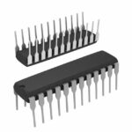 MC14067BCP

The activity of extra discounts on wholesale prices is in full swing…
Please fill in your contact information and we will send you the latest wholesale price list.





