 ChipApex | Global Electronic Components Supplier

SEARCH
Search Product
Search Post
— IC芯片 | 连接器 | 传感器 | 被动器件 —
Search productSearch post
— IC芯片 | 连接器 | 传感器 | 被动器件 —
Consult the customer manager about the wholesale price.
consultation hotline:86-132-6715-2157
email:[email protected]
Contact the product manager for consultation. One-stop consultation is available.
Do you want a lower wholesale price? Please send us your inquiry and we will reply immediately.
MC145027DWR2 is listed in the Encoders, Decoders, Converters range at ChipApex. The manufacturer field lists NXP USA Inc.. Its product description is IC DECODER 5 ADDR 4 DATA 16-SOIC. Review the specifications below when checking this part for your BOM.
The MC145027DWR2 is a CMOS decoder integrated circuit manufactured by NXP USA Inc., designed for use in remote control applications. It operates within a supply voltage range of 4.5V to 18V and features a 16-SOIC surface-mount package with a width of 7.50mm. The device interprets five trinary address digits, allowing for 243 unique addresses, while processing four bits of binary data. It includes an internal power-on reset that forces all outputs low upon initialization.
Verify component authenticity through official manufacturer channels due to discontinued status. Confirm RoHS compliance requirements as the datasheet indicates non-compliance. Check for moisture sensitivity level 2 classification and ensure proper storage conditions are maintained prior to assembly.
Select this decoder when paired with the MC145026 encoder for systems requiring five-bit trinary addressing. Ensure the application voltage remains between 4.5V and 18V. Consider the SC41343 variant if operation below 4.5V is required, noting its specific low-voltage characteristics.
Part of the MC145026/27/28 family of CMOS encoder-decoder pairs originally developed by Motorola. The DWR2 suffix denotes a tape-and-reel packaging format suitable for automated surface-mount assembly processes. This series is widely recognized for low standby current and robust noise immunity in consumer electronics.
SC41343 is a verified low-voltage replacement operating from 2.8V to 10V. Direct pin-compatible alternatives may include other MC145027 variants with different suffixes indicating package type changes, provided voltage ratings align with system requirements.
The Valid Transmission (VT) output remains low if a mismatch occurs in either the address or data bits during the two-word sequence. VT also disables if no signal is received for four data periods.
Pins R1 and C1 accept external resistor and capacitor components to set the time constant for pulse discrimination, determining whether a received pulse is interpreted as a logic high or low.
Yes, while it supports trinary addressing, the four data bits must be binary (logic 0 or 1). A trinary open state on the encoder's data lines is decoded as a logic high by the receiver.
Explore related parts through Interface, Integrated Circuits (ICs), all product categories, ChipApex homepage.
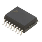 MC145027DWR2

The activity of extra discounts on wholesale prices is in full swing…
Please fill in your contact information and we will send you the latest wholesale price list.





