 ChipApex | Global Electronic Components Supplier

SEARCH
Search Product
Search Post
— IC芯片 | 连接器 | 传感器 | 被动器件 —
Search productSearch post
— IC芯片 | 连接器 | 传感器 | 被动器件 —
Consult the customer manager about the wholesale price.
consultation hotline:86-132-6715-2157
email:[email protected]
Contact the product manager for consultation. One-stop consultation is available.
Do you want a lower wholesale price? Please send us your inquiry and we will reply immediately.
The MC74HC4066ADTR2 is a quad analog switch manufactured by onsemi using silicon-gate CMOS technology. It features four independent bilateral switches capable of controlling analog and digital voltages across the full power-supply range from VCC to GND. The device operates with a supply voltage between 2.0 V and 12.0 V and supports an operating temperature range from -55°C to +125°C. Key electrical parameters include a maximum ON resistance of 120 Ω at 4.5 V, propagation delays ranging from 10 ns to 80 ns depending on voltage, and a bandwidth up to 160 MHz. It is housed in a TSSOP-14 package.
Verify the specific ordering suffix to confirm the package type and tape/reel specifications. Confirm RoHS compliance and Pb-Free status as indicated by the 'G' suffix or microdot marking. Ensure the automotive '-Q' suffix is present if AEC-Q100 qualification and PPAP capability are required for the application.
Select this component for applications requiring low ON resistance and high linearity across a wide voltage range. Consider the TSSOP-14 package for surface-mount assembly. Evaluate the propagation delay requirements against the supply voltage, as delays vary significantly between 2.0 V and 12.0 V. Ensure unused I/O pins are terminated to minimize crosstalk.
This device belongs to the HC4066A series of quad analog switches. It is pin-compatible with older metal-gate CMOS devices like the MC14016 and MC14066 but offers superior performance characteristics due to its silicon-gate construction. The ADTR2 designation specifically indicates the SOIC-14 or TSSOP-14 package variant with tape and reel packaging.
MC74HC4066ADR2G
The maximum ON resistance decreases as the supply voltage increases. At 4.5 V, it is guaranteed at 70 Ω, while at 2.0 V, it can be as high as 120 Ω. Operation near 3 V may exhibit non-linear behavior.
Unused analog inputs and outputs may be left floating, but it is advisable to tie them to VCC or GND through a low-value resistor to minimize crosstalk and feedthrough noise pickup.
Yes, the ON/OFF control inputs are compatible with LSTTL outputs when external pull-up resistors (typically 2 to 10 kΩ) are used.
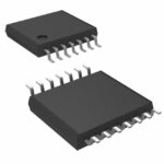 MC74HC4066ADTR2

The activity of extra discounts on wholesale prices is in full swing…
Please fill in your contact information and we will send you the latest wholesale price list.





