 ChipApex | Global Electronic Components Supplier

SEARCH
Search Product
Search Post
— IC芯片 | 连接器 | 传感器 | 被动器件 —
Search productSearch post
— IC芯片 | 连接器 | 传感器 | 被动器件 —
Consult the customer manager about the wholesale price.
consultation hotline:86-132-6715-2157
email:[email protected]
Contact the product manager for consultation. One-stop consultation is available.
Do you want a lower wholesale price? Please send us your inquiry and we will reply immediately.
MC74HC595AMN1TWG-Q is listed in the Shift Registers range at ChipApex. The manufacturer field lists onsemi. Its product description is SHIFT REGISTER 3-STATE. Review the specifications below when checking this part for your BOM.
The MC74HC595AMN1TWG-Q is an 8-bit serial-input/serial or parallel-output shift register with latched 3-state outputs. It consists of an 8-bit shift register and an 8-bit D-type latch. The device operates within a voltage range of 2.0 to 6.0 V, supports an operating temperature from -55°C to +125°C, and features a maximum propagation delay of 225 ns at 6.0 V. It utilizes a QFN-16 package.
Verify that the specific ordering suffix MN1TWG-Q corresponds to the QFN-16 package and tape & reel shipping configuration as listed in the official datasheet. Confirm compliance with AEC-Q100 qualification standards and PPAP capability requirements before finalizing procurement specifications.
Select this component when an 8-bit shift register with latched 3-state outputs is required for space-constrained designs due to its QFN-16 footprint. Ensure the application environment falls within the specified -55°C to +125°C temperature range and operates between 2.0 V and 6.0 V supply voltages.
This part belongs to the MC74HC595A family of high-performance silicon-gate CMOS logic devices. It offers improvements over standard HC595/HCT595 devices, including improved propagation delays, lower quiescent power consumption, and enhanced input noise and latchup immunity.
MC74HC595ADG-Q
The Output Enable pin is active-low; a low signal allows data from the latches to be presented at the outputs, while a high signal forces the outputs into a high-impedance state.
The Reset input is active-low and asynchronous. A low signal resets only the shift register portion of the device, leaving the 8-bit latch unaffected.
Explore related parts through Logic, Integrated Circuits (ICs), all product categories, ChipApex homepage.
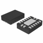 MC74HC595AMN1TWG-Q

The activity of extra discounts on wholesale prices is in full swing…
Please fill in your contact information and we will send you the latest wholesale price list.





