 ChipApex | Global Electronic Components Supplier
MC74LCX125DR2G
Search Product
Search Post
— IC芯片 | 连接器 | 传感器 | 被动器件 —
Search productSearch post
— IC芯片 | 连接器 | 传感器 | 被动器件 —
Consult the customer manager about the wholesale price.
consultation hotline:86-132-6715-2157
email:[email protected]
Contact the product manager for consultation. One-stop consultation is available.
Do you want a lower wholesale price? Please send us your inquiry and we will reply immediately.
The MC74LCX125DR2G is a quad buffer and line driver manufactured by onsemi, belonging to the 74LCX logic family. It features four non-inverting buffers with three-state outputs, designed for low-voltage operation between 2.0 V and 3.6 V. The device utilizes advanced silicon-gate CMOS technology to achieve high-speed performance while maintaining low power consumption. It is housed in a 14-SOIC package and supports surface-mount installation. Key electrical characteristics include a propagation delay of 9 ns at 3.3 V and 7 ns at 5 V, with output drive capabilities of 24 mA for both high and low states.
Verify the specific ordering suffix DR2G to confirm the SOIC-14 package and tape-and-reel quantity. Ensure the component meets RoHS compliance requirements for your assembly process. Cross-reference the manufacturer part number with authorized distributors to avoid counterfeit sources. Confirm that the voltage levels in your target application remain within the specified 2.0 V to 3.6 V operating range for reliable functionality.
Select this component when designing circuits that require multiple buffered outputs with tri-state capability in a compact surface-mount form factor. It is suitable for applications demanding low supply voltage operation and moderate speed performance. Consider the 14-pin SOIC footprint for PCB layout constraints. Compare against other LCX series variants if different pin counts or inversion types are required for the specific design topology.
This part belongs to the 74LCX series of low-voltage CMOS logic devices from onsemi. The LCX family is engineered for high-speed operation with reduced power consumption compared to older HC or HCT technologies. It serves as a standard solution for level shifting and buffering in modern digital electronics where 3.3 V logic levels are prevalent.
Compatible substitutes include the NXP SN74LCX125D and Texas Instruments SN74LCX125D. Verify pinout compatibility and electrical specifications before substitution. Ensure the alternative part supports the same 3.3 V operating voltage and three-state output functionality.
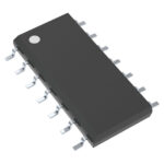 MC74LCX125DR2G
The activity of extra discounts on wholesale prices is in full swing…
Please fill in your contact information and we will send you the latest wholesale price list.





