 ChipApex | Global Electronic Components Supplier
MC74LCX16240DTR2
Search Product
Search Post
— IC芯片 | 连接器 | 传感器 | 被动器件 —
Search productSearch post
— IC芯片 | 连接器 | 传感器 | 被动器件 —
Consult the customer manager about the wholesale price.
consultation hotline:86-132-6715-2157
email:[email protected]
Contact the product manager for consultation. One-stop consultation is available.
Do you want a lower wholesale price? Please send us your inquiry and we will reply immediately.
The MC74LCX16240DTR2G is a low-voltage CMOS 16-bit buffer with 5 V-tolerant inputs and outputs. It operates from a 2.3 V to 3.6 V supply and features inverting, 3-state outputs controlled by four independent Output Enable (OEn) inputs for nibble control. The device provides balanced output sink and source capability of 24 mA at VCC = 3.0 V to 3.6 V. Propagation delay ranges from 1.5 ns to 5.4 ns depending on voltage and load conditions. Quiescent supply current is near zero across all logic states.
Verify the specific ordering suffix 'DTR2G' corresponds to the TSSOP-48 package and tape & reel shipping configuration. Confirm RoHS compliance and Pb-free status as indicated by the 'G' suffix. Ensure the procurement quantity aligns with the standard factory pack size of 2500 units per tape and reel.
Select this component for designs requiring 16-bit buffering between 2.3 V to 3.6 V logic domains and 5.0 V systems. The independent OEn pins allow flexible nibble-level control without tying all enables together. Verify that the required propagation delay fits within the system timing constraints under the specific operating voltage and capacitive load conditions.
This part belongs to the MC74LCX series of low-voltage CMOS logic devices manufactured by onsemi. It is functionally similar to other 16-bit buffers but specifically designed for 5 V tolerance and high drive current. The device replaces older 5 V only buffers in mixed-voltage systems where power consumption and signal integrity are critical.
MC74LCX16240MTCXG
The MC74LCX16240 supports live insertion and withdrawal due to its IOFF specification, which ensures outputs remain in a high impedance state when VCC is 0 V.
Yes, the device is nibble-controlled with four separate Output Enable inputs (OE1-OE4). These can be tied together for full 16-bit operation or used independently to control groups of four outputs.
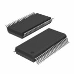 MC74LCX16240DTR2
The activity of extra discounts on wholesale prices is in full swing…
Please fill in your contact information and we will send you the latest wholesale price list.





