 ChipApex | Global Electronic Components Supplier

SEARCH
Search Product
Search Post
— IC芯片 | 连接器 | 传感器 | 被动器件 —
Search productSearch post
— IC芯片 | 连接器 | 传感器 | 被动器件 —
Consult the customer manager about the wholesale price.
consultation hotline:86-132-6715-2157
email:[email protected]
Contact the product manager for consultation. One-stop consultation is available.
Do you want a lower wholesale price? Please send us your inquiry and we will reply immediately.
The MC74LVX4051DT is an analog multiplexer/demultiplexer manufactured by onsemi, utilizing high-performance silicon-gate CMOS technology. It features a single-pole eight-throw (SP8T) configuration with three digital channel-select inputs and an active-high enable input. The device operates within a digital power supply range of 2.5 V to 6.0 V and supports analog signals across the complete supply range from VCC to VEE. Key electrical parameters include a maximum propagation delay of 40 ns at 2.5 V, a maximum ON resistance of 86 Ω at 3.0 V, and a bandwidth of 80 MHz. It is housed in a TSSOP-16 package.
Verify the specific ordering suffix DT corresponds to the TSSOP-16 package when sourcing components. Confirm RoHS compliance status as required by project specifications. Ensure that the supply voltage limits are strictly adhered to during operation to maintain device reliability and prevent damage to the internal CMOS structures.
Select this component when a single 8-channel analog switch is required with low distortion and high isolation. The LVX series offers better linearity than standard HC or HCT families. Consider the TSSOP-16 package constraints regarding thermal dissipation and board space. Verify that the control logic voltage levels are compatible with the 2.5 V to 6.0 V operating range.
This device belongs to the MC74LVX4051 family of analog multiplexers. It shares pinout compatibility with devices such as the LVX8051, HC4051A, and MC14051B. The DT suffix specifically denotes the Thin Shrink Small Outline Package (TSSOP) with 16 leads, distinguishing it from SOIC or SOEIAJ variants within the same functional family.
MC74LVX4051D
When the Enable pin is HIGH, all analog switches are turned off, placing the outputs in a high-impedance state regardless of the channel-select inputs.
Yes, the device can be designed to operate using split supplies up to ±3.0 V, provided the difference between VCC and VEE remains within the 2.5 V to 6.0 V range.
Unused analog inputs/outputs may be left floating, but tying them to VCC or GND through a low-value resistor helps minimize crosstalk and feedthrough noise.
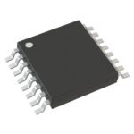 MC74LVX4051DT

The activity of extra discounts on wholesale prices is in full swing…
Please fill in your contact information and we will send you the latest wholesale price list.





