 ChipApex | Global Electronic Components Supplier
MC74LVX50DT
Search Product
Search Post
— IC芯片 | 连接器 | 传感器 | 被动器件 —
Search productSearch post
— IC芯片 | 连接器 | 传感器 | 被动器件 —
Consult the customer manager about the wholesale price.
consultation hotline:86-132-6715-2157
email:[email protected]
Contact the product manager for consultation. One-stop consultation is available.
Do you want a lower wholesale price? Please send us your inquiry and we will reply immediately.
The MC74LVX50DT is a hex buffer fabricated with advanced high-speed silicon gate CMOS technology. It operates within a supply voltage range of 2.0 V to 3.6 V and features inputs that tolerate voltages up to 5.5 V, enabling interface between 5.0 V and 3.0 V systems. The device provides balanced propagation delays and low noise characteristics. At VCC = 3.3 V, the typical propagation delay is 4.1 ns with a 15 pF load. Quiescent supply current is typically 2 µA at 25°C.
Verify the specific ordering suffix against the manufacturer's documentation to confirm package type and shipping quantity. The base model designation may correspond to multiple packaging options such as tape and reel or tube. Confirm RoHS compliance status and lead time requirements directly with authorized distributors prior to procurement.
Select this component when interfacing different voltage domains is required without level shifting circuitry. The wide input voltage tolerance simplifies system design by allowing direct connection to higher voltage sources. Ensure the operating temperature range meets environmental specifications and verify that the package dimensions fit the target PCB layout constraints.
This device belongs to the MC74LVX series of advanced CMOS logic components designed for low-voltage applications. The LVX family offers improved performance over standard CMOS technologies while maintaining compatibility with legacy logic interfaces. It serves as a fundamental building block for digital logic designs requiring buffering and signal integrity.
MC74LVX50DR2G
No, unused inputs must not be left open. They must be tied to a high- or low-logic input voltage level to ensure proper functionality.
The inputs tolerate DC voltages up to 5.5 V, allowing safe interfacing with 5.0 V systems even when the device is powered at lower voltages.
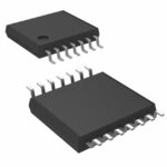 MC74LVX50DT
The activity of extra discounts on wholesale prices is in full swing…
Please fill in your contact information and we will send you the latest wholesale price list.





