 ChipApex | Global Electronic Components Supplier
MC74LVX541DWG
Search Product
Search Post
— IC芯片 | 连接器 | 传感器 | 被动器件 —
Search productSearch post
— IC芯片 | 连接器 | 传感器 | 被动器件 —
Consult the customer manager about the wholesale price.
consultation hotline:86-132-6715-2157
email:[email protected]
Contact the product manager for consultation. One-stop consultation is available.
Do you want a lower wholesale price? Please send us your inquiry and we will reply immediately.
The MC74LVX541DWG is an octal bus buffer fabricated with advanced high-speed CMOS technology. It operates within a supply voltage range of 2.0 V to 3.6 V and features noninverting outputs controlled by two independent output enable inputs (OE1, OE2). The device provides balanced propagation delays and high noise immunity. Inputs tolerate voltages up to 5.5 V, enabling interface between 5.0 V systems and 3.0 V systems. It is housed in a 20-pin SOIC package.
Verify the specific ordering suffix 'DWG' corresponds to the SOIC-20 package and lead-free status. Confirm the manufacturer part number matches the datasheet exactly. Ensure the component meets RoHS compliance requirements for your assembly process. Check for any specific handling instructions related to moisture sensitivity level.
Select this component for applications requiring octal buffering with dual independent control. It is suitable for designs needing voltage translation from 5.0 V inputs to 3.3 V or 2.5 V systems. Consider its low quiescent current and high noise immunity for signal integrity in noisy environments. Verify package availability if space constraints require surface-mount installation.
This part belongs to the LVX series of advanced high-speed CMOS logic devices. It is functionally compatible with other standard logic families but optimized for lower voltage operation. The octal configuration allows for efficient data bus management in complex digital systems.
MC74LVX541DTR2G: TSSOP-20 package variant with identical electrical characteristics and pinout.
The inputs can tolerate DC voltages up to 5.5 V, allowing safe interfacing with 5.0 V logic systems even when the device is powered at lower voltages like 3.3 V.
Unused outputs should be left open. Unused inputs must always be tied to an appropriate logic voltage level, either GND or VCC, to ensure proper operation.
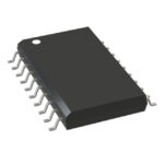 MC74LVX541DWG
The activity of extra discounts on wholesale prices is in full swing…
Please fill in your contact information and we will send you the latest wholesale price list.





