 ChipApex | Global Electronic Components Supplier

SEARCH
Search Product
Search Post
— IC芯片 | 连接器 | 传感器 | 被动器件 —
Search productSearch post
— IC芯片 | 连接器 | 传感器 | 被动器件 —
Consult the customer manager about the wholesale price.
consultation hotline:86-132-6715-2157
email:[email protected]
Contact the product manager for consultation. One-stop consultation is available.
Do you want a lower wholesale price? Please send us your inquiry and we will reply immediately.
The MC74LVXT8053DTR2 is a Triple Single-Pole, Double-Position Plus Common Off analog multiplexer/demultiplexer manufactured by onsemi. It utilizes high-performance silicon-gate CMOS technology to achieve fast propagation delays and low ON resistances. The device supports an analog power supply range of 2.0 V to 6.0 V and features independent control of three switches (X, Y, Z). Key electrical parameters include a maximum ON resistance of 25 Ω at 5.5 V, a bandwidth of 120 MHz, and a propagation delay of 2.0 ns from analog input to output at 5.5 V. It operates within a temperature range of -55°C to +85°C.
Verify the package suffix 'DTR2' corresponds to the TSSOP-16 form factor before procurement. Confirm that the specific revision level matches the design requirements, as datasheet revisions may update electrical characteristics or pin configurations. Ensure compatibility with the required operating temperature range of -55°C to +85°C for the intended application environment.
Select this component when requiring triple SPDT switching with low crosstalk and high bandwidth. It is suitable for applications needing interface between different logic voltage levels due to its robust input protection. Consider the TSSOP-16 package constraints if space is limited. Verify that the analog signal swing remains within the 2.0 V to 6.0 V supply range to ensure proper operation.
This part belongs to the MC74LVXT8053 family of analog multiplexers. It shares functional similarities with the HC4053A and MC14053B but offers enhanced performance through silicon-gate CMOS technology. The 'DTR2' suffix specifically denotes the Tape & Reel packaging in the TSSOP-16 case, distinguishing it from SOIC or SOEIAJ variants.
Direct replacements include MC74LVXT8053DR2G (SOIC-16) and MC74LVXT8053M (SOEIAJ-16), provided the package footprint is adaptable. Other LVXT series multiplexers may serve as functional substitutes if pinout and electrical specifications align with the design requirements.
The device provides protection circuitry that allows overvoltage tolerance on the inputs up to 7.0 V, regardless of the supply voltage.
The ON resistance decreases as the supply voltage increases; for example, it is guaranteed at a maximum of 25 Ω at 5.5 V and 40 Ω at 3.0 V.
Yes, unused analog inputs and outputs may be left floating, though tying them to VCC or GND through a low-value resistor can help minimize crosstalk and feedthrough noise.
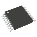 MC74LVXT8053DTR2

The activity of extra discounts on wholesale prices is in full swing…
Please fill in your contact information and we will send you the latest wholesale price list.





