 ChipApex | Global Electronic Components Supplier

SEARCH
Search Product
Search Post
— IC芯片 | 连接器 | 传感器 | 被动器件 —
Search productSearch post
— IC芯片 | 连接器 | 传感器 | 被动器件 —
Consult the customer manager about the wholesale price.
consultation hotline:86-132-6715-2157
email:[email protected]
Contact the product manager for consultation. One-stop consultation is available.
Do you want a lower wholesale price? Please send us your inquiry and we will reply immediately.
The MC74VHC4051DR2G is a single-pole, eight-position analog multiplexer/demultiplexer manufactured by onsemi using silicon-gate CMOS technology. It operates with a digital supply voltage (VCC) ranging from 2.0 V to 6.0 V and an analog supply range (VCC - VEE) of 2.0 V to 12.0 V. The device features a maximum ON resistance of 100 Ω at VCC = 6.0 V and a bandwidth of 80 MHz. Propagation delays are specified at 45 ns for channel-select to output transitions at VCC = 6.0 V. It is housed in a SOIC-16 package.
Verify the specific ordering suffix 'DR2G' corresponds to the SOIC-16 package and tape-and-reel shipping configuration. Confirm RoHS compliance and Pb-free status as indicated by the manufacturer's documentation. Ensure the component matches the required operating temperature range of -55°C to +125°C for the intended application environment.
Select this component when a single-channel, eight-input multiplexing function is required within a 2V to 6V logic domain. Consider the 100 Ω ON resistance and 80 MHz bandwidth limits for signal integrity requirements. Verify that the analog signal swing remains within the VCC to VEE supply rails to ensure proper switch operation and avoid excessive current draw.
This part belongs to the MC74VHC405x family, which includes the dual 4-to-1 (MC74VHC4052) and triple 2-to-1 (MC74VHC4053) variants. All devices share identical pinouts and utilize the same silicon-gate CMOS process. The family is designed as a drop-in replacement for older HC4051A and MC14051B series devices while offering enhanced performance characteristics.
Direct pin-compatible replacements include the MC74VHC4051DTR2G in TSSOP-16 packaging. Automotive-grade alternatives with the NLV prefix, such as NLVVHC4051DTR2G, are available for applications requiring AEC-Q100 qualification. Older metal-gate equivalents like the MC14051B offer functional compatibility but differ in electrical specifications.
The analog input voltage can vary across the complete power supply range, from VEE to VCC.
When the Enable pin is HIGH, all analog switches are turned off, placing the outputs in a high-impedance state.
No, the ON resistance varies with the input voltage, but it is more linear than metal-gate CMOS switches. Maximum values are specified at endpoints and midpoints.
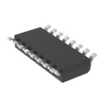 MC74VHC4051DR2G

The activity of extra discounts on wholesale prices is in full swing…
Please fill in your contact information and we will send you the latest wholesale price list.





