 ChipApex | Global Electronic Components Supplier

SEARCH
Search Product
Search Post
— IC芯片 | 连接器 | 传感器 | 被动器件 —
Search productSearch post
— IC芯片 | 连接器 | 传感器 | 被动器件 —
Consult the customer manager about the wholesale price.
consultation hotline:86-132-6715-2157
email:[email protected]
Contact the product manager for consultation. One-stop consultation is available.
Do you want a lower wholesale price? Please send us your inquiry and we will reply immediately.
The MC74VHC4053DTR2G is a high-performance silicon-gate CMOS analog multiplexer/demultiplexer manufactured by onsemi. It integrates three independent single-pole double-throw (SPDT) switches within a 16-pin TSSOP package. The device operates with a digital supply voltage (VCC to GND) ranging from 2.0 V to 6.0 V and supports an analog power supply range (VCC to VEE) of 2.0 V to 12.0 V. Key electrical characteristics include a maximum ON resistance of 100 Ω at VCC = 6.0 V, a -3 dB bandwidth of 120 MHz, and low off-channel leakage current of 1.0 μA maximum. Propagation delays are specified at 75 ns maximum for channel select to output at VCC = 2.0 V.
Verify the specific ordering suffix 'DTR2G' corresponds to the TSSOP-16 package and tape-and-reel shipping configuration. Confirm RoHS compliance and Pb-free status as indicated by the 'G' suffix. Ensure the component meets the required operating temperature range of -55°C to +125°C for the intended application environment.
Select this component when multiple independent analog channels require switching within a compact surface-mount footprint. The wide analog supply range allows control of signals varying across the complete power supply range. Consider the 100 Ω ON resistance and 120 MHz bandwidth for signal integrity requirements in high-speed applications.
This part belongs to the MC74VHC405x family of analog multiplexers, which includes the MC74VHC4051 (8-channel) and MC74VHC4052 (4-channel). These devices share pinout compatibility with the older HC4051A/52A/53A series and metal-gate MC14051B/52B/53B counterparts, facilitating direct upgrades for improved linearity and lower ON resistance.
Publicly confirmed substitute part numbers include MC74VHC4053DR2G (SOIC-16 package variant) and NLVVHC4053DTR2G (automotive qualified variant). Verify package dimensions and pinout compatibility before substitution.
The device controls analog voltages that may vary across the complete power supply range from VCC to VEE, with a total analog supply range (VCC - VEE) of up to 12.0 V.
When the Enable pin is HIGH, all analog switches are turned off, placing the outputs in a high-impedance state regardless of the channel-select inputs.
Yes, the device is designed so that the ON resistance (Ron) is more linear over the input voltage than metal-gate CMOS analog switches, improving signal fidelity.
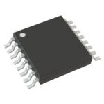 MC74VHC4053DTR2G

The activity of extra discounts on wholesale prices is in full swing…
Please fill in your contact information and we will send you the latest wholesale price list.





