 ChipApex | Global Electronic Components Supplier

SEARCH
Search Product
Search Post
— IC芯片 | 连接器 | 传感器 | 被动器件 —
Search productSearch post
— IC芯片 | 连接器 | 传感器 | 被动器件 —
Consult the customer manager about the wholesale price.
consultation hotline:86-132-6715-2157
email:[email protected]
Contact the product manager for consultation. One-stop consultation is available.
Do you want a lower wholesale price? Please send us your inquiry and we will reply immediately.
MC74VHC595DTR2G-Q is listed in the Shift Registers range at ChipApex. The manufacturer field lists onsemi. Its product description is IC SHIFT REGISTER 3-ST 16TSSOP. Review the specifications below when checking this part for your BOM.
The MC74VHC595DTR2G-Q is an 8-bit shift register with an output storage register and 3-state outputs, fabricated using silicon gate CMOS technology. It operates within a voltage range of 2.0 V to 5.5 V and supports temperatures from -55°C to +125°C. The device features independent Shift Clock (SCK) and Register Clock (RCK) inputs, allowing parallel outputs to remain stable during shifting. It achieves a maximum clock frequency of 185 MHz at 5 V and includes power-down protection on inputs.
Verify that the ordering suffix '-Q' is correctly specified, as it denotes automotive qualification and unique site/control change requirements distinct from standard commercial variants. Confirm the package type matches the required footprint, specifically TSSOP-16 for this part number. Ensure compliance with RoHS standards and lead-free specifications before finalizing procurement orders.
Select this component when interface compatibility between 5 V and 3 V systems is required, given its input tolerance up to 5.5 V. Choose the MC74VHC595DTR2G-Q over standard versions if the application demands AEC-Q100 qualification and PPAP capability. Consider the 3-state output feature if bus sharing is necessary in the design architecture.
This device belongs to the MC74VHC595 series of advanced high-speed logic components. It is functionally compatible with other standard logic families while offering improved performance metrics typical of the VHC family. The '-Q' designation indicates specific manufacturing controls for automotive and rigorous industrial applications.
Standard commercial equivalents such as MC74VHC595DTR2G lack the '-Q' suffix and associated automotive qualifications. Cross-reference with Nexperia's 74AHC595PW-Q100,11 for similar functionality, but verify pinout and electrical parameter alignment carefully.
They allow the contents of the shift register to be transferred to the storage register without affecting the parallel outputs, keeping them stable during the shift operation.
The inputs are designed with power-down protection to prevent excessive current flow when the supply voltage is removed or below operating levels.
Explore related parts through Logic, Integrated Circuits (ICs), all product categories, ChipApex homepage.
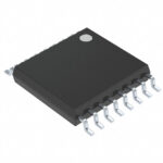 MC74VHC595DTR2G-Q

The activity of extra discounts on wholesale prices is in full swing…
Please fill in your contact information and we will send you the latest wholesale price list.







