 ChipApex | Global Electronic Components Supplier

SEARCH
Search Product
Search Post
— IC芯片 | 连接器 | 传感器 | 被动器件 —
Search productSearch post
— IC芯片 | 连接器 | 传感器 | 被动器件 —
Consult the customer manager about the wholesale price.
consultation hotline:86-132-6715-2157
email:[email protected]
Contact the product manager for consultation. One-stop consultation is available.
Do you want a lower wholesale price? Please send us your inquiry and we will reply immediately.
MC74VHCT259ADTRG is listed in the Latches range at ChipApex. The manufacturer field lists onsemi. Its product description is IC LATCH/DECODER/SHIFTER 16TSSOP. Review the specifications below when checking this part for your BOM.
The MC74VHCT259ADTRG is an 8-bit addressable latch fabricated with silicon gate CMOS technology, housed in a TSSOP-16 package. It operates within a DC supply voltage range of 4.5 V to 5.5 V and supports an operating temperature range from -55°C to +125°C. The device features TTL-compatible inputs with a maximum quiescent supply current of 40 µA at 5.5 V. Propagation delays vary by input source: data-to-output delay is typically 6.0 ns at 5.0 V with 15 pF load; address-select-to-output delay is typically 6.0 ns (15 pF) or 8.5 ns (50 pF); enable-to-output delay is typically 6.0 ns (15 pF) or 8.5 ns (50 pF); and reset-to-output delay is typically 6.0 ns (15 pF) or 8.5 ns (50 pF).
Verify component status before procurement as the MC74VHCT259ADTRG is officially marked as discontinued in the datasheet revision history dated August 5, 2026. Confirm availability through authorized representatives and ensure replacement strategies are in place for ongoing production requirements.
Select this component for designs requiring 8-bit addressable latching with LSTTL-compatible inputs and wide industrial temperature ranges. Ensure the application utilizes the recommended 4.5 V to 5.5 V supply voltage. Note that changing more than one bit of the address should be performed only while the device is in memory mode to avoid transient wrong addresses.
This device belongs to the VHCT logic family, combining high-speed CMOS operation with low power dissipation similar to Bipolar Schottky TTL. It is functionally compatible with other standard logic families but offers enhanced noise immunity and power-down protection characteristics specific to the VHCT architecture.
Consult onsemi representatives for current alternatives due to discontinuation status. Cross-reference with MC74VHCT259ADR2G (SOIC-16) or MC74VHCT259ADG (SOIC-16 tube) if package compatibility allows, though these are also listed as discontinued in the provided documentation.
Changing more than one bit of the address can impose a transient wrong address. This operation should only be performed while the device is in memory mode to prevent unintended state changes.
The VHCT inputs are compatible with TTL levels, specifically VIL = 0.8 V and VIH = 2.0 V, allowing it to interface with LSTTL logic standards.
Explore related parts through Logic, Integrated Circuits (ICs), all product categories, ChipApex homepage.
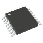 MC74VHCT259ADTRG

The activity of extra discounts on wholesale prices is in full swing…
Please fill in your contact information and we will send you the latest wholesale price list.





