 ChipApex | Global Electronic Components Supplier

SEARCH
Search Product
Search Post
— IC芯片 | 连接器 | 传感器 | 被动器件 —
Search productSearch post
— IC芯片 | 连接器 | 传感器 | 被动器件 —
Consult the customer manager about the wholesale price.
consultation hotline:86-132-6715-2157
email:[email protected]
Contact the product manager for consultation. One-stop consultation is available.
Do you want a lower wholesale price? Please send us your inquiry and we will reply immediately.
MC74VHCT373ADTR2G is listed in the Latches range at ChipApex. The manufacturer field lists onsemi. Its product description is OCTAL TRANSPARENT LATCH 3-STATE. Review the specifications below when checking this part for your BOM.
The MC74VHCT373ADTR2G is an octal D-type latch with 3-state output fabricated using silicon gate CMOS technology. It operates within a supply voltage range of 4.5 V to 5.5 V and supports an operating temperature from -40°C to +85°C. The device features a maximum propagation delay of 8.5 ns at 5.0 V with a 50 pF load, a typical quiescent supply current of 4 µA, and output drive capabilities of 8 mA for both high and low states. It is housed in a TSSOP-20 package.
Verify the specific ordering suffix 'DT' corresponds to the TSSOP-20 package configuration required for your PCB layout. Confirm that the 'G' suffix indicates a lead-free, halogen-free, and RoHS-compliant component status. Ensure the manufacturer part number matches exactly to avoid functional differences associated with other series variants like the standard VHC version.
Select this component when TTL-compatible inputs are necessary alongside CMOS low-power characteristics. It is suitable for designs requiring 3-state outputs for bus sharing. Verify that the 4.5 V minimum supply voltage aligns with the system power rails. Consider the TSSOP-20 package dimensions against available board space constraints.
This device belongs to the MC74VHCT373A family of advanced high-speed CMOS octal latches. It is functionally compatible with standard logic families but offers improved speed and lower power consumption compared to equivalent Bipolar Schottky TTL devices. The VHCT series specifically bridges the gap between CMOS and TTL logic levels.
MC74VHCT373ADWR2G (SOIC-20 variant)
The device inputs are compatible with TTL levels, allowing it to interface 3.3 V systems to 5.0 V systems while providing full 5.0 V CMOS level output swings.
The output structures provide protection when VCC = 0 V, helping prevent device destruction caused by supply voltage-input/output voltage mismatch, battery backup, or hot insertion.
Explore related parts through Logic, Integrated Circuits (ICs), all product categories, ChipApex homepage.
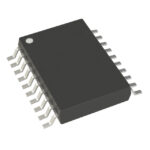 MC74VHCT373ADTR2G

The activity of extra discounts on wholesale prices is in full swing…
Please fill in your contact information and we will send you the latest wholesale price list.





