ChipApex | Global Electronic Components Supplier

SEARCH
Search Product
Search Post
— IC芯片 | 连接器 | 传感器 | 被动器件 —
Search productSearch post
— IC芯片 | 连接器 | 传感器 | 被动器件 —
Consult the customer manager about the wholesale price.
consultation hotline:86-132-6715-2157
email:[email protected]
Contact the product manager for consultation. One-stop consultation is available.
Do you want a lower wholesale price? Please send us your inquiry and we will reply immediately.
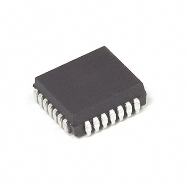
MC88915FN55 is listed in the Clock Generators, PLLs, Frequency Synthesizers range at ChipApex. The manufacturer field lists NXP USA Inc.. Its product description is IC CLOCK DRIVER 28PLCC. Review the specifications below when checking this part for your BOM.
The MC88915FN55 is a PLL-based clock driver designed for high-performance PC and workstation applications. It locks low-skew outputs to an input reference clock, providing zero-delay distribution or frequency multiplication (2X). The device features five Q outputs (Q0–Q4) with less than 500 ps skew, an inverted Q5 output, a 2X_Q output running at twice the Q frequency, and a Q/2 output. It operates within a supply voltage range of 4.75V to 5.25V. The maximum operating frequency for the 2X_Q output is 55 MHz, while the Q outputs are limited to 27.5 MHz.
Verify the manufacturer origin, as this component was originally produced by Motorola and later acquired by NXP USA Inc. Confirm the specific suffix 'FN' corresponds to the 28-pin PLCC package (Case 776-02). Ensure the FN55 variant matches the required 55 MHz maximum frequency specification for the 2X_Q output.
Select the MC88915FN55 when the application requires a maximum 2X_Q frequency of 55 MHz. If higher frequencies up to 70 MHz are needed, consider the MC88915FN70 variant. Ensure the design accommodates the 5.0V ±5% power supply requirement and provides adequate bypass capacitance (0.1μF and 10μF) near the analog pins to minimize jitter.
The MC88915 belongs to the Motorola/NXP 88915 series of timing solutions. It is part of a family that includes variants like the MC88915FN70. The device utilizes Yield Surface Modeling (YSM) for performance guaranteeing. It is distinct from general-purpose logic drivers due to its integrated VCO and charge pump loop filter interface.
Public confirmed substitute part numbers include MC88915FN70 for higher frequency requirements. Other manufacturers such as IDT and NXP list similar PLL clock drivers in the 88915 series, but direct functional equivalence must be verified against the specific electrical characteristics and pinout compatibility.
The RC1 pin is used for the external loop filter network. A 470kΩ resistor tied to Analog VCC or Analog GND is required to prevent jitter and inject current into the internal charge pump.
The FREQ_SEL pin selects between divide-by-1 and divide-by-2 in the PLL feedback path. Holding it high (÷1) is standard; holding it low (÷2) allows the VCO to run optimally (>20 MHz) when using low-frequency reference inputs.
No. The LOCK output should only be used for passive monitoring or evaluation. Under certain conditions, it may remain low even when phase-locked, making it unsuitable for driving active circuits.
Explore related parts through Clock/Timing, Integrated Circuits (ICs), all product categories, ChipApex homepage.
 MC88915FN55

The activity of extra discounts on wholesale prices is in full swing…
Please fill in your contact information and we will send you the latest wholesale price list.